 FDCE/FDPE/FDRE/FDSE触发器简介
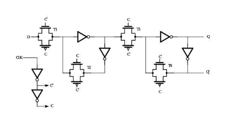
每个 Slice 有 8 个 FF 。四个可以配置为 D 型触发器或电平敏感锁存器,另外四个只能配置为 D 型触发器,但是需要记得是:当原来的四个 FF 配置为锁存器时,不能使用这四个 FF 。
FDCE
简介
带有时钟使能和异步清零的 D 触发器
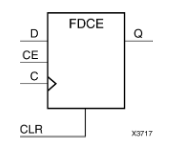
-
当时钟使能(CE)为高并且异步清零信号 CLR 为低时,该 D 触发器将数据输入 D 端传递到输出 Q 端。
-
当CLR为高,不管输入是什么,输出 Q 端值为 0。
原语
FDCE #(.INIT(1'b0) // Initial value of register (1'b0 or 1'b1)) FDCE_inst (.Q(Q), // 1-bit Data output.C(C), // 1-bit Clock input.CE(CE), // 1-bit Clock enable input.CLR(CLR), // 1-bit Asynchronous clear input.D(D) // 1-bit Data input);
真值表
FDPE
简介
带有时钟使能和异步置位的 D 触发器
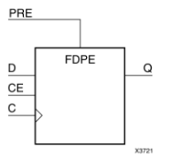
-
当时钟使能(CE)为高并且异步置位信号 PRE 为低时,该 D 触发器将数据输入 D 端传递到输出 Q 端。
-
当 PRE 为高,不管输入是什么,输出 Q 端值为 1。
原语
FDPE #(.INIT(1'b0) // Initial value of register (1'b0 or 1'b1)) FDPE_inst (.Q(Q), // 1-bit Data output.C(C), // 1-bit Clock input.CE(CE), // 1-bit Clock enable input.PRE(PRE), // 1-bit Asynchronous preset input.D(D) // 1-bit Data input);
真值表
FDRE
简介
带有时钟使能和同步清零的 D 触发器
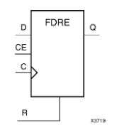
-
当时钟使能(CE)为高并且同步清零信号 R 为低时,该 D 触发器在时钟上升沿将数据输入 D 端传递到输出 Q 端。
-
当 R 为高,不管输入是什么,输出 Q 端值为 0。
原语
FDRE #(.INIT(1'b0) // Initial value of register (1'b0 or 1'b1)) FDRE_inst (.Q(Q), // 1-bit Data output.C(C), // 1-bit Clock input.CE(CE), // 1-bit Clock enable input.R(R), // 1-bit Synchronous reset input.D(D) // 1-bit Data input);
真值表
FDSE
简介
带有时钟使能和同步置位的 D 触发器
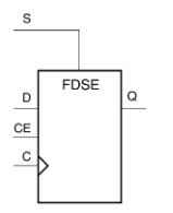
-
当时钟使能(CE)为高并且同步置位信号 S 为低时,该 D 触发器在时钟上升沿将数据输入 D 端传递到输出 Q 端。
-
当 S 为高,不管输入是什么,输出 Q 端值为 1。
原语
FDSE #(.INIT(1'b0) // Initial value of register (1'b0 or 1'b1)) FDSE_inst (.Q(Q), // 1-bit Data output.C(C), // 1-bit Clock input.CE(CE), // 1-bit Clock enable input.S(S), // 1-bit Synchronous set input.D(D) // 1-bit Data input);
真值表
原文标题:参考链接
文章出处:【微信公众号:FPGA之家】欢迎添加关注!文章转载请注明出处。
声明:本文内容及配图由入驻作者撰写或者入驻合作网站授权转载。文章观点仅代表作者本人,不代表电子发烧友网立场。文章及其配图仅供工程师学习之用,如有内容侵权或者其他违规问题,请联系本站处理。
举报投诉
-
时钟
+关注
关注
11文章
1750浏览量
131937 -
锁存器
+关注
关注
8文章
918浏览量
41706 -
触发器
+关注
关注
14文章
2024浏览量
61414
原文标题:参考链接
文章出处:【微信号:zhuyandz,微信公众号:FPGA之家】欢迎添加关注!文章转载请注明出处。
发布评论请先 登录
相关推荐
硬件描述语言(HDL)编码技术:xilinx verilog语法技巧
and Registers : Vivado综合根据HDL代码的编写方式推断出四种类型的寄存器原语: •FDCE:具有时钟使能和异步清除的D触发器 •FDPE:具有时钟使能和异步预设
JK触发器,JK触发器是什么意思
JK触发器,JK触发器是什么意思
1.主从JK触发器主从结构触发器也可以彻底解决直接控制,防止空翻。这里以性能优良、广泛使用的主从JK触发器
发表于 03-08 13:36
•6911次阅读
施密特触发器,施密特触发器是什么意思
施密特触发器,施密特触发器是什么意思
施密特触发器也有两个稳定状态,但与一般触发器不同的是,施密特触发器采用电位
发表于 03-08 14:14
•1993次阅读
教你们怎么去设定寄存器的初始值
对于寄存器,如果没有明确指定其初始值,Vivado会根据其类型(FDCE/FDRE/FDPE/FDRE)设定合适的初始值。有些工程师喜欢使用

FPGA——LUT/FDRE/FDCE/FDSE/FDPE
因为当输入数据的位数远大于一个LUT的输入时,就需要用多个LUT级联来实现逻辑,那么级联产生的延时也就不可避免了,这样就会制约系统的运行频率。那么为了避免级联数过于多,就采用插入寄存器的方法来实现
触发器的触发顺序是什么
不同类型的触发器可能有不同的执行顺序。例如,对于同一个表上的多个触发器,插入触发器(INSERT trigger)可能先于更新触发器(UPDATE trigger)执行。
t触发器和jk触发器的区别和联系
触发器是数字电路中常用的组合逻辑电路,在现代电子系统中有着广泛的应用。其中,最常用的两种触发器是T触发器和JK触发器。本文将详细介绍T触发器
t触发器变为d触发器的条件
在数字电路设计中,触发器是一种非常重要的存储元件,用于存储一位二进制信息。触发器的种类很多,其中最为常见的有JK触发器、D触发器和T触发器等
d触发器和jk触发器的区别是什么
引言 数字电路是现代电子技术的基础,广泛应用于计算机、通信、控制等领域。触发器是数字电路中的一种基本逻辑元件,具有存储和传递信息的功能。 触发器的基本概念 触发器是一种具有记忆功能的数字电路元件
怎么用jk触发器变成t触发器
将JK触发器变成T触发器,主要涉及到对JK触发器的输入端口进行适当的连接和配置,以实现T触发器的逻辑功能。以下是将JK触发器转换为T


 工商网监
工商网监
评论