ADI公司的ADGS1408/ADGS1409是包含有八个单路和四个差分通路的模拟复接器,SPI接口控制模拟开关,具有很好的误差检测特性如循环冗余检查(CRC)误差检测,无效读/写地址检测,以及SCLK计数误差检测。支持突发模式和菊花链模式,工作电压±15 V,±5 V和+12 V,25℃时的开态电阻4Ω,主要用在自动测试设备(ATE),数据采集系统,通信系统,取样和保持系统,音频信号路由,视频信号路由,电池为能源系统,以及继电器替代品。本文介绍了ADGS1408/ADGS1409产品亮点和主要特性,功能框图,以及EVAL-ADGS1408SDZ/EVAL-ADGS1409SDZ主要特性,电路图,材料清单和PCB设计图。
The ADGS1408/ADGS1409 are analog multiplexers comprising eight single channels and four differential channels, respectively. A serial peripheral interface (SPI) controls the switches. The SPI interface has robust error detection features such as cyclic redundancy check (CRC) error detection, invalid read/write address detection, and SCLK count error detection. It is possible to daisy-chain multiple ADGS1408/ADGS1409 devices together. Daisy-chain mode enables the configuration of multiple devices with a minimal amount of digital lines. The ADGS1408/ADGS1409 can also operate in burst mode to decrease the time between SPI commands. iCMOS construction ensures ultra low power dissipation, making the devices ideally suited for portable and battery-powered instruments. Each switch conducts equally well in both directions when on, and each switch has an input signal range that extends to the supplies. In the off condition, signal levels up to the supplies are blocked. The on-resistance profile is flat over the full analog input range, which ensures linearity and low distortion when switching audio signals.
ADGS1408/ADGS1409产品亮点:
1. SPI interface removes the need for parallel conversion, logic traces, and reduces GPIO channel count.
2. Daisy-chain mode removes additional logic traces when multiple devices are used.
3. CRC error detection, invalid read/write address detection, and SCLK count error detection ensure a robust digital interface.
4. CRC and error detection capabilities allow the use of the ADGS1408/ADGS1409 in safety critical systems. 5. Minimal distortion.
ADGS1408/ADGS1409主要特性:
SPI interface with error detection
Includes CRC, invalid read/write address, and SCLK count error detection
Supports burst mode and daisy-chain mode
Industry-standard SPI Mode 0 and SPI Mode 3 interface compatible
Round robin mode allows switching times comparable with a parallel interface
General-purpose digital outputs to control other devices, such as parallel switches from Analog Devices, Inc.
4 Ω typical on resistance at 25℃
0.5 Ω typical on-resistance flatness at 25℃
0.2 Ω typical on-resistance match between channels at 25°C VSS to VDD analog signal range
Fully specified at ±15 V, ±5 V, and +12 V
Power-up sequence of VDD, VSS, and GND before applying VL and digital/analog inputs
1.8 V logic compatibility with 2.7 V ≤ VL ≤ 3.3 V
24-lead LFCSP package
ADGS1408/ADGS1409应用:
Automated test equipment
Data acquisition systems
Battery-powered systems
Sample-and-hold systems
Audio signal routing
Video signal routing
Communications systems
Relay replacement

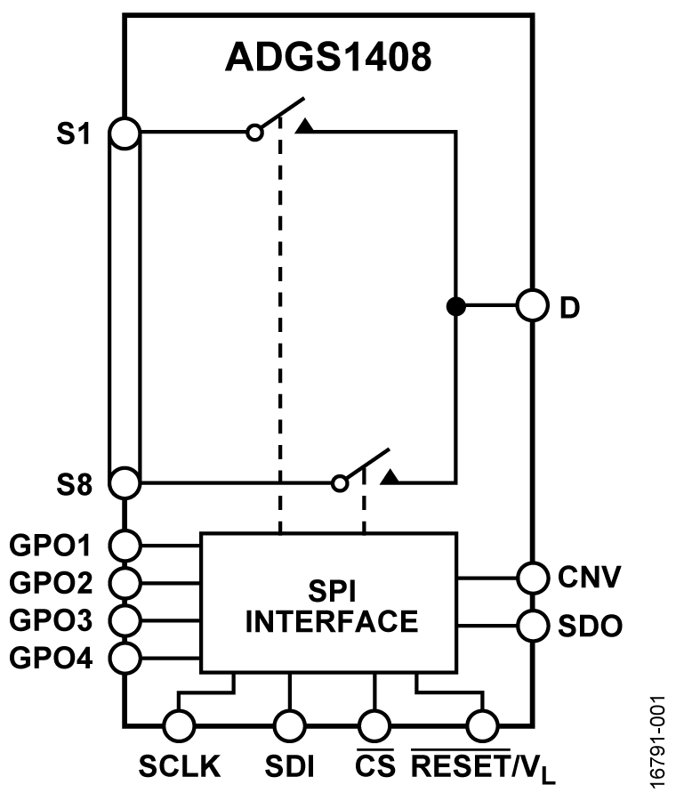
图1.ADGS1408功能框图

图2.ADGS1409功能框图

图3.ADGS1408控制ADG758电路图
评估板EVAL-ADGS1408SDZ/EVAL-ADGS1409SDZ
The EVAL-ADGS1408SDZ/EVAL-ADGS1409SDZ are theevaluation boards for the ADGS1408/ADGS1409. TheADGS1408/ADGS1409 are low RON, 8:1/dual 4:1 multiplexerscontrolled by a serial peripheral interface (SPI)。 The SPI has robust error detection features, including cyclic redundancy check (CRC) error detection, invalid read/write addressdetection, and serial clock (SCLK) count error detection. It ispossible to daisy-chain multiple ADGS1408/ADGS1409 devicestogether to enable the configuration of multiple devices with aminimal amount of digital lines. The ADGS1408/ADGS1409also support burst mode, which decreases the time between SPI commands. Figure 1 and Figure 2 shows the EVAL-ADGS1408SDZ/EVAL-ADGS1409SDZ board photographs. The EVAL-ADGS1408SDZ/ EVAL-ADGS1409SDZ are controlled by the EVAL-SDP-CB1Zsystem demonstration platform (SDP), which connects to a PC via a USB port. The ADGS1408/ADGS1409 is on the center of the evaluation board, and wire screw terminals are provided to connect to each of the source and drain pins. Three screwterminals power the device and, if required, a fourth terminal provides users with a defined digital logic supply voltage.
Alternatively, the digital logic supply voltage can be supplied from the SDP-B board. Consult the ADGS1408/ADGS1409 data sheet (available from Analog Devices, Inc.) in conjunction with this user guide when working with the evaluation board. The evaluation board interfaces to the USB port of a PC via the SDP-B board. The SDP-B controller board (EVAL-SDP-CB1Z)is available for order at
EVAL-ADGS1408SDZ/EVAL-ADGS1409SDZ主要特性:
SPI interface with error detection
Includes CRC error detection, invalid read/write addressdetection, and SCLK count error detection Analog supply voltages
Dual supply: ±15 V Single supply: 12 V PC control in conjunction with evaluation software EVALUATION KIT CONTENTS EVAL-ADGS1408SDZ/EVAL-ADGS1409SDZ
图4.EVAL-ADGS1408SDZ外形图
图5.EVAL-ADGS1409SDZ外形图

图6.EVAL-ADGS1408SDZ电路图-主器件(1)

图7.EVAL-ADGS1408SDZ电路图-主器件(2)

图8.EVAL-ADGS1408SDZ电路图-电源和硬件重置

图9.EVAL-ADGS1408SDZ电路图-SDP连接器

图10.EVAL-ADGS1408SDZ PCB设计图-丝印

图11.EVAL-ADGS1408SDZ PCB设计图-顶层

图12.EVAL-ADGS1408SDZ PCB设计图-层2

图13.EVAL-ADGS1408SDZ PCB设计图-层3

图14.EVAL-ADGS1408SDZ PCB设计图-底层

图15.EVAL-ADGS1409SDZ电路图-主器件(1)

图16.EVAL-ADGS1409SDZ电路图-主器件(2)

图17.EVAL-ADGS1409SDZ电路图-电源和硬件重置

图18.EVAL-ADGS1409SDZ电路图-SDP连接器
EVAL-ADGS1408/9SDZ材料清单:


图19.EVAL-ADGS1409SDZ PCB设计图-丝印

图20.EVAL-ADGS1409SDZ PCB设计图-顶层

图21.EVAL-ADGS1409SDZ PCB设计图-层2

图22.EVAL-ADGS1409SDZ PCB设计图-层3

图23.EVAL-ADGS1409SDZ PCB设计图-底层
-
ADI
+关注
关注
146文章
45821浏览量
250190 -
SPI接口
+关注
关注
0文章
258浏览量
34387
发布评论请先 登录
相关推荐
请问有大神可以指点设计一个多路PCM编码的复接器
ADI最新中文资料(2018年1月)
【限时下载】ADI 用于多路抽头输出隔离电源的简易解决方案
采用SPI接口的模拟开关提高通道密度
多路复用与数字复接
ADGS1408 SPI 接口 4 Ω RON, ±15 V/+12 V/±5 V、 1.8 V 逻辑控制 8:1 多路复用器

ADGS1412:SPI接口,</SUB>上1.5ΩR<SUB>,±15 V/+12 V,四路单通道开关,多路复用器可配置数据表

UG-1284:评估ADGS1408/ADGS1409SPI接口,4ΩRON,±15 V/+12 V/±5 V,1.8V逻辑控制,8:1/双4:1复用器

EVAL-ADGS1408-1409 EVAL-ADGS1408-1409评估板
ADGS1408/ADGS1409模拟多路复用器中文手册


 ADI ADGS1408(9)SPI接口多路复接器解决方案


评论