How to Calibrate the MAX9979 Pin Electronics
Abstract: The MAX9979 Pin Electronics device integrates 28 DACs, that can be calibrated to adjust for gain and offset errors. Calibration is done with the MAX9979's calibration registers. This calibration will result in a very linear and precise driver/PMU/comparator/active-load that will meet the most stringent demands of the tester industry.
Introduction
The MAX9979 is a highly linear, dual, 1.1Gbps pin electronics with integrated PMU and level-setting digital-to-analog converters (DACs). The device integrates a total of twenty-eight 16-bit DACs (14 per channel). Each of these DACs feeds levels can be independently adjusted for gain and offset errors by using the device's calibration registers. These registers allow the MAX9979 levels to be calibrated to better than 5mV over the entire -1.5V to +6.5V operating range. This application note will explain how this calibration can be accomplished.
Gain and Offset Errors in Buffers
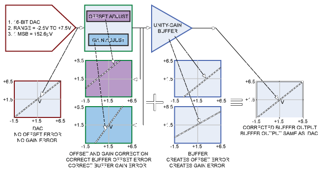
There are a number of unity-gain buffers inside the MAX9979. Each of these buffers, if not corrected, will exhibit offset and gain errors. Figure 1 shows how one of these buffers looks like in the MAX9979.
Figure 1. MAX9979 level-setting architecture.
The internal 16-bit DAC output drives the input of the offset and gain correction cell, which corrects the offset and gain errors of the unity-gain buffer. It is this architecture that creates high precision, linear, low-offset levels over the MAX9979's entire operating range.
The MAX9979 data sheet explains the offset and gain calibration registers, as well as how to address and program these registers with the internal serial interface. The following section illustrates how this calibration is accomplished using the MAX9979 EV (evaluation) kit. The MAX9979 EV kit provides both visual and actual results (Figure 2).
Calibrating MAX9979 Using the MAX9979 EV Kit
Figure 2. The MAX9979 EV kit.
The EV kit, as shown above, is controlled by a graphics user interface (GUI) that can be downloaded from the Maxim website:
Setting Up the MAX9979 EV Kit Board
- Power up EV kit board by following the instructions in the EV kit manual.
- Connect the DATA0 pin to 0.8V.
- Connect the DATA0/ pin to 0V.
- Connect the RCV0 pin to 0V.
- Connect the RCV0/ pin to 0.8V.
- Connect a high-precision DVM to the DUT0 pin.
- Load the GUI software.
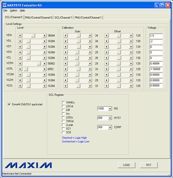
With the above setup, we are ready to begin the calibration. At startup the GUI interface should look like Figure 3.
Figure 3. MAX9979 GUI at startup.
Click on the DriveHi CH1/CH0 quickstart. Observe and verify that you are measuring 3V with the DVM attached to the DUT0 pin.
Procedure to Calibrate VDH0
- Offset Adjustment
Always adjust the offset before the gain.- Click in the voltage cell for VDH0 and reset to 1.5V. This will set the DUT0 output to +1.5V, which is the midpoint between the -1.5V < VDH0 < +6.5V operating range. Set VDL0 to -2.0V to ensure that there is at least a 0.5V difference between VDH0 and VDL0 as VDH0 approaches VDL0.
- Monitor the voltage at the DUT node with the DVM. This will not be 1.5V, but will be offset from the 1.5V.
- Adjust the offset slider for VDH0 in either direction until the DUT's measured voltage is as close to the programmed voltage of 1.5V. Once this is done you have programmed the offset correction voltage in the MAX9979's internal calibration register for VDH0. There is no further need to adjust or move the offset slider.
- Gain Adjustment
There are many places to set VDH0 to calibrate the gain adjustment. You could set VDH0 to -1.5V, adjust the gain slider, then set VDH0 to +6.5V and check the measured voltage. However, there are nonlinearities at the extremes of the range. The biggest linearity error occurs when VDH0 is approaching VDL0.
A better approach is to always operate the device in the most linear region. In this case we will operate within ±1.5V of the setting of VDH0.- VDL0 is set to -2V. Keep the offset calibration as previously set in the offset adjustment steps above.
- Set VHD0 to 0V (-1.5V away from the original setting).
- Observe the DUT measurement. Adjust the gain slider (leaving the offset slider undisturbed) until the DUT's output is as close to 0V as possible.
- Set VDH0 to 3V (+1.5V above the original setting) and observe the DUT's voltage.
- The reading should now be very close to 3.000V. Our pivot point was picked to be +1.5V and the gain adjusted for ±1.5V around this pivot point. If the reading at VDH = 3V has more error than desired (it should be less than 2mV at this point), then repeat steps 2 through 5 to get a symmetrical error at 0V and 3V.
- Once this is finalized, run a sweep of VDH0 from -1.5V to +6.5V. Plot the error difference between the programmed voltage and measured voltage.
After setting VDH0 = +1.5V, VDL0 = -2V, and after calibrating the offset and the gain, the GUI interface appears as in Figure 4. The VDH0 offset and gain settings may differ from that shown, since they depend on the particular device being tested.
Figure 4. Setting for VDH0 offset and gain registers after calibration.
VDH Error Sweep Before and After Calibration
Note from Figure 5:
- The offset before the calibration procedure was:
- -1.5V = -27mV
- +1.5V = +5mV
- +6.5V = +54mV
- The offset after the calibration procedure was:
- -1.5V = -3mV
- +1.5v = -0.1mV
- +6.5V = +0.1mV
The error at -1.5V is related to VDH0 approaching VDL0. The calibration points for the gain could have been chosen to be closer to -1.5V and closer to +6.5V. If that was done, there would be less error at -1.5V and slightly more error along the swept curve up to +6.5V.
This procedure is repeated for every level, for both channels. To calibrate the comparator offsets you will need to monitor the comparator outputs and look for the switching points, or place the comparators in a servo loop with external components.
Figure 5. Measured DVH (typ) error at the DUT0 pin before and after calibration.
Saving the Calibration Register Settings
After calibrating all the registers, the GUI interface may look similar to Figure 6, where all the offset and gain registers are set to their calibrated values. The DAC values for the levels other than VDH0, which was calibrated, are assumed; these numbers will be updated depending on the calibration of your device.
Note that we are just looking at the CH0 page, but that there are three other pages in the GUI setup for the CH0 PMU settings and the CH1 driver and PMU settings. When a full calibration is done, then all the offset and gain DAC settings will be shown on all the GUI pages.
These settings only remain while the MAX9979 is powered up. If the MAX9979 is powered down and then powered up again, all of these calibrated register settings will be lost. The startup default values will reappear.
These registers were updated, in this case, by programming the serial interface. The end user will also need to program these calibration constants into the MAX9979 after a power-up sequence by using the serial interface. Therefore, it is important to store these constants in a table and read this table back into the MAX9979 registers at each power-up.
The EV kit can store these constants in a saved file. The user simply clicks on the "File" pulldown menu, clicks on "Save," names a file, and then defines the location where to store this file. Now the user can click on the "File" pulldown menu after power-up, and click on the "Load" option. Browse to the location to load the saved calibration file and the MAX9979 will be fully calibrated, ready for use.
The "Save" and "Load" options in the "File" pulldown menu can also be used to store any setup, which can include the calibration constants. With this capability you can upload one setup after another, simplifying the characterization of your MAX9979.
Figure 6. Typical offset and gain settings after calibration.
Summary
You can calibrate the MAX9979 levels, supplied by its internal 16-bit DACs, by adjusting the offset and gain bits per each DAC. This calibration will result in a very linear and precise driver/PMU/comparator/active-load that will meet the most stringent demands of the tester industry. All of this capability has been integrated in the MAX9979 pin electronics device.
By using the methodology discussed here and by reviewing the MAX9979 data sheet, you will be able to test, characterize, and utilize all the capabilities of the device.
 电子发烧友App














评论