The DS2409 is designed for use in access-control probe points (i.e., readers) and to lower the bus load in large
Introduction
With its unique feature set, the DS2409 MicroLAN coupler can be used in a several specialized applications. This application note first lists the features and applications of the DS2409 and then identifies alternative circuits that can be used to achieve comparable functionality. Subsequently, the alternative circuits are discussed in more detail.
DS2409 Description
The DS2409 is a special type of a 2-port addressable switch. Instead of switching a programmable input/output (PIO) to high or low, the part connects its output ports to the incoming 1-Wire line using transmission gates. No more than a single 1-Wire output can be active at any given time. Besides the 1-Wire outputs, the DS2409 has a control output which can be associated with the main output (default), the auxiliary output, or be operated independently. This configuration is controlled through the Status Control Byte (see data sheet). The Status Info Byte (see data sheet) allows the master to verify the device configuration, and to check the status (active or inactive), the logic state (high or low), and the event flag (set/cleared) of each 1-Wire output. Table 1 summarizes these and additional features and explains their benefits.
Table 1. DS2409 Features and Benefits
| Feature Name | Description | Benefits |
| No more than one output active at any time | Only one output can be connected to the incoming |
Keeps the bus load low. |
| Control output | The DS2409 has an open-drain control output. On power-up, the control output is configured to light an LED when the main output is active. Under software control, the control output can be associated to the auxiliary output or be turned on/off directly. | Automatically indicates the active channel. Can also be used to implement a handshaking function, as shown in the Dual-master network example below. |
| Event detection | Both outputs have an event-detection feature. If the output is inactive, a falling edge on the output, e.g., caused by a presence pulse of an arriving 1-Wire slave, sets the event flag. | Latching an event lowers bus traffic. |
| Conditional search | If the event flag of the main output is set, the part participates in the conditional search. | Reduces bus traffic in an access-control application. |
| Reset pulse before output activation | Both outputs assert a reset pulse before activation (see Smart-On commands, Table 4). | Reduces communication overhead when opening a path through a multilayer network. |
| Short detection | Both outputs have a short detection feature (see Smart-On commands). | Prevents bus collapse due to short or sabotage. |
The DS2409 requires a 5V VDD supply for operation. On power-up, both the 1-Wire outputs are inactive and pulled to VDD through internal resistors. A short power-supply disconnect causes the part to perform a power-on reset. With VDD power available, a short disruption of the incoming 1-Wire line causes the DS2409 to perform a soft power-on reset. When the master is reconnected, the configuration is reset to its power-on default state and the 1-Wire outputs are inactive; the state of the event flags is undefined.
The features in Table 1 are targeted towards the three main applications: a smart probe point, multilayer network, and dual-master network (see Table 2).
Table 2. Features vs. Application Matrix
Smart Probe Point
Figure 1 shows the topology of an access-control system that uses iButton® devices as electronic keys. The combination R1/C1 should be included near the 1-Wire adapter. R1 is needed to ensure that the DS2409s perform a soft power-on reset if the 1-Wire bus is interrupted. C1 prevents the DS2409s from obstructing the 1-Wire bus in case of a VDD outage.

Figure 1. Access-control topology with smart probe points.
Instead of the main 1-Wire bus, the probe points (e.g., DS9092 iButton probe) are located on secondary network that branches off the main output of a DS2409. Connected to the auxiliary output is an ID chip, e.g., a 1-Wire EEPROM programmed with the branch name. During normal operation, all the branches are inactive (disconnected from the main bus) while the host computer performs a conditional search to detect events. An iButton that arrives at one of the probe points sets the event flag of the DS2409 that controls the branch. With the next scan cycle, the host locates the DS2409 and activates the auxiliary output to read the branch name. Next, the host accesses the same DS2409 and activates the main output to communicate with the iButton that has just arrived. While the main output is active, the LED is on, confirming to the user that the arrival is detected. Instead of lighting an LED, the control output could be wired to unlock the door under software control. Due to the short detection of the Smart-On command, the DS2409 prevents the network from failure if the probe is shorted.
Multilayer Network
For any network it is important to find the best balance between the load that the master must drive and the number of nodes (or braches, or slaves) serviced. One method to achieve this is a multilayer topology (Figure 2). The illustration shows four layers, beginning with the trunk (Layer 0), which is always active. Every subsequent layer consists of switched branches (Layers 1 to 3). The combination R1/C1 should be included near the 1-Wire master. If a path through one or more DS2409 devices is established and the connection between the 1-Wire trunk and master breaks, R1 ensures that the path is automatically switched off when the master is reconnected. C1 prevents the DS2409s from obstructing the 1-Wire bus in case of a VDD outage.
To efficiently control such a network, the master should know the network's topology in the form of the ROM ID numbers of all DS2409 slaves on each branch on each layer. To open the path to slaves on Layer 3, as indicated by the turquoise arrow, the master would have to issue the following command sequence:
- Match ROM for U1 on the trunk.
- Activate the main output (this opens the path to two slaves on Layer 1).
- Match ROM for U3 on Layer 1.
- Activate the main output (this opens the path to two slaves on Layer 2).
- Match ROM for U4 on Layer 2.
- Activate the auxiliary output (this opens the path to the slaves on Layer 3 that are connected to this output).

Figure 2. Multilayer network topology.
As a VCC-powered device, the DS2409 loads the 1-Wire bus with 100pF, maximum (50pF from the 1-Wire input and 50pF from the activated output). For comparison, a typical parasitically powered 1-Wire slave adds a load of 800pF to 1000pF. In this example topology, the total load that the master must drive is: one DS2409 on the trunk (50pF), two DS2409s on Layer 1 (150pF, two inputs, one output), two DS2409s on Layer 2 (150pF), all slaves connected to the auxiliary port of U4 (50pF + slaves). This is a total 400pF plus slaves.
Depending on the requirements of the application, there could be more than two DS2409s on each branch. Table 3 shows the maximum number of branches created and the corresponding load from the couplers. From layer to layer, the number of branches grows exponentially, while the load from the DS2409 increases only linearly.
Table 3. Multilayer Branches Created vs. DS2409 Load
| Network Depth | Configuration | |||
| Two DS2409s per Branch | Three DS2409s per Branch | Four DS2409s per Branch | ||
| Layer 0 | Branches created | 4 | 6 | 8 |
| Total DS2409 load | Two parts | Three parts | Four parts | |
| Layer 1 | Branches created | 16 | 36 | 64 |
| Total DS2409 load | Four parts | Six parts | Eight parts | |
| Layer 2 | Branches created | 64 | 216 | 512 |
| Total DS2409 load | Six parts | Nine parts | 12 parts | |
| Layer 3 | Branches created | 256 | 1296 | 4096 |
| Total DS2409 load | Eight parts | 12 parts | 16 parts | |
| Layer n | Branches created | 4 × 4n | 6 × 6n | 8 × 8n |
| Total DS2409 load | 2 × n + 2 | 3 × n + 3 | 4 × n + 4 | |
Besides the communication overhead to open the path to the destination layer, which increases linearly with the number of layers, one also needs to consider the impedance that the DS2409 adds to the path. For the main output, this is typically 10Ω (20Ω, max), and typically 15Ω (30Ω, max) for the auxiliary output. The overall effect of the nonzero impedance reduces the high-level voltage on the destination layer (master-to-slave) and raises the low-level voltage at the trunk (slave-to-master). The reduced high level is generally not an issue. However, due to the raised low level one should not go beyond Layer 4.
Dual-Master Network
There could be situations where two masters need to control a 1-Wire network, e.g., as backup or to exchange data with each other. Figure 3 shows a circuit to accomplish this. In this example, the DS1996 memory iButton serves as a temporary storage for the data packets to be exchanged. The ID chips are optional. If installed, they could store system-specific data telling the hosts that they are accessing a shared network with storage buffer and handshaking logic. Besides the memory iButton there could be a network of 1-Wire slaves. The R1/C1 combination shown in Figure 1 is also recommended for the dual-master application; it should be included on both sides.
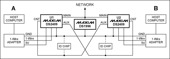
Figure 3. Dual-master concept. If identical voltage cannot be guaranteed, power both DS2409 devices from the same source.
As a starting condition, the main outputs and the auxiliary outputs of both DS2409s are inactive. The shared network is pulled to 5V from both DS2409s, thus lowering the effective pullup resistor to 750Ω. Both hosts regularly read the status information of their DS2409 to know whether the other host has taken control over the 1-Wire network.
Assume now that host A wants to access the DS1996 to send a message to host B. To access the memory iButton (DS1996), host A first activates the control output of U1, which pulls the auxiliary output of U2 low. Host B, meanwhile, has been reading the U2 status information and therefore knows that host A has taken over. Next, host A activates the main output of coupler U1 and writes data to the memory iButton. When finished writing, host A deactivates the main output of U1 and deactivates the control output.
Host B, still reading the U2 status information, realizes that host A has finished writing. Now, host B activates the control output of U2, which pulls the auxiliary output of U1 low. Host A reads the U1 status information and therefore knows that host B has taken over. Host B now activates the main output of U2 and reads the message from the memory iButton. After processing the message, host B writes a response to the iButton. When finished, host B deactivates the main output of U2 and deactivates the control output. Host A, still reading the U1 status information, knows that host B's access has ended.
Function Commands and Their Typical Use
The DS2409 understands a total of 11 commands, which implement either network functions or control functions. Table 4 lists these commands and indicates their purpose and typical use. The commands are sorted by their importance in a network application. For more details, refer to the DS2409 data sheet.
Table 4. DS2409 Function Commands and Their Typical Use
| Command Name | Function | Purpose | Typical Use |
| Match ROM | Network | Selecting a single 1-Wire slave | The main addressing mode |
| Smart-On Main | Control | Activating the main output with test for presence pulse and short | Cautious output activation, e.g., with the intention of a subsequent Match ROM to open the path to the next layer |
| Smart-On Auxiliary | Control | Activating the auxiliary output with test for presence pulse and short | Cautious output activation, e.g., with the intention of a subsequent Match ROM to open the path to the next layer |
| Skip ROM | Network | Addressing all 1-Wire slaves on the active branches of the network | To broadcast a command, e.g., All Lines Off |
| All Lines Off | Control | Clearing event flags; output deactivation; termination of Discharge Lines command | After a Skip ROM command: disconnecting the current path; general network reset without changing any configuration |
| Status Read/Write | Control | Read: verifying output status and configuration; Write: device configuration |
Read: output level sensing (e.g., handshake in the dual-master concept); event flag testing (smart probe point); verifying configuration and which output is active Write: changing the mode and association of the control output; direct operation of the control output. |
| Conditional Search ROM | Network | Identifying 1-Wire slaves on the active branches of the network that need attention | Detecting the arrival of an iButton at a smart probe point |
| Search ROM | Network | Identifying all 1-Wire slaves on the active branches of the network | Determining the topology of the network; creating an inventory of all slaves in the network. |
| Discharge Lines | Control | Powering down both outputs | Power-on reset of parasitically powered slaves connected to both outputs; network troubleshooting |
| Direct-On Main | Control | Activating the main output | Fast output activation |
| Read ROM | Network | Reading the ROM ID | (Not useful in a multiple slave network) |
Particularly interesting is the Smart-On command (Figure 4). The top trace shows the communication of the incoming 1-Wire bus, which is a Smart-On Auxiliary command in this example. The first byte is the command code 33h, followed by the reset stimulus FFh, the reset response (00h, = presence pulse detected), and the confirmation byte (33h, = no short). The center trace shows the activity on the auxiliary output, i.e., a reset/presence detect (PD) cycle. The bottom trace shows the transition at the Control output, as the main output is deactivated prior to the activation of the auxiliary output. Any communication after the confirmation byte is passed through to the activated output. The presence pulse reporting is correct only if preceded by an All Lines Off command.
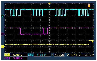
Figure 4. Smart-On Auxiliary command.
The normal way to deactivate an output is through the All Lines Off command (Figure 5). The top trace shows the command byte 66h, followed by the confirmation byte. While the command byte is passed through to the output (center trace), the confirmation byte is not. The bottom trace shows the control output, as it changes with the deactivation of the output.
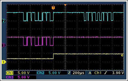
Figure 5. All Lines Off command.
Besides the Smart-On, there is a Direct-On command for the main output (Figure 6). The scope traces look just like a mirror image of the All Lines Off command. Immediately after the command code A5h, the main output is activated (bottom trace). The confirmation byte is passed through to the output (center trace). If this command is used, a reset/PD cycle must follow to ensure that the slaves on the activated output are synchronized with the master.
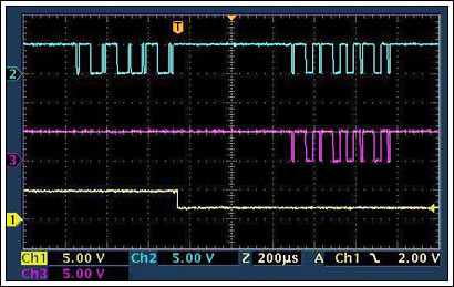
Figure 6. Direct-On Main command.
DS2409 Emulation
To emulate a DS2409 one needs 1-Wire addressable switches (for digital control and sensing) and analog switches (to activate or deactivate the outputs). A partial emulation is possible with a 2-channel addressable switch (e.g., DS2413, DS2406, or DS28E04) plus one or two analog switches. For a full emulation one needs a 5-channel 1-Wire addressable switch (e.g., DS2408, 8 channels) plus two analog switches. It is important that the addressable switch powers up with all PIOs in an off (nonconducting) state.
The analog switch must be of the single-pole/double-throw (SPDT) type. When selecting a switch, look for a supply voltage of 5V ±10%, an on-resistance (RON) of 30Ω or less, and low capacitance (no more than 50pF) on all three nodes of the switch. The turn-on and turn-off time should not exceed 100ns. Excellent built-in ESD protection is desirable. Based on data sheet specifications, the following analog switches were identified as suitable:
- Single-channel: MAX4729 (5.7Ω, max), MAX4730 (5.7Ω, max), MAX4644 (4.75Ω, max)
- Dual-channel: MAX4717 (3.5Ω, max), MAX4719 (25Ω, max), MAX4635 (4.5Ω, max), MAX4636 (4.5Ω, max), MAX4750 (30Ω, max)
- Triple-channel: MAX4693 (25Ω, typical, 40Ω, max; slow switching).
None of the above switches has good ESD protection. The bench tests were conducted using the MAX4561 single-channel switch, which has built-in ESD protection of ±15kV at the NO and NC pins. Particularly due to its high RON value of typically 45Ω, the MAX4561 should not be considered for DS2409 emulation.
Example Circuits
The example circuit in Figure 7 is a partial emulation that implements one switched 1-Wire output and the control output of the DS2409. U1 is the 2-channel 1-Wire addressable switch with open-drain PIO ports. U2 is the SPDT analog switch. The three switch terminals occupy pins NO, NC, and COM. The switch is controlled by the digital level at the IN pin.
In the power-on default state, both PIOs of the 1-Wire addressable switch are in high impedance. Resistor R2 applies a logic-high to the switch's IN pin, which causes the NO pin to be connected to COM. Resistor R1 at the NO pin provides the 1.5kΩ pullup to the inactive 1-Wire output at the COM pin. This is equivalent to the power-on state of the DS2409.
To activate the 1-Wire output of U2, the master turns PIO-A on, which applies a logic-low to the IN pin of U2. This causes the analog switch to disconnect COM from NO and to connect it to NC, i.e., the incoming 1-Wire bus. Turning PIO-A off deactivates the 1-Wire output. The master can operate PIO-B independently of PIO-A, e.g., to emulate the DS2409's control output in manual mode or to control another R1/R2/U2-like circuit. When controlling two analog switches, the 1-Wire master must ensure that no more than one 1-Wire output is activated. This can be done through software or (safer) with the help of glue logic that decodes the cases PIO-A ^ active-low PIO-B and active-low PIO-A ^ PIO-B to control the analog switches. PIO-B could also be used for event detection (conditional search) and short detection (dotted line). A reset pulse before output activation cannot be supported.
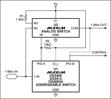
Figure 7. Partial DS2409 emulation circuit . U1 could be a DS2406, DS2413 or DS28E04.
DS2406 Addressable Switch
The circuit of Figure 7 has been tested using the DS2406 addressable switch. The IN pin of the analog switch (MAX4561) was connected to PIO-B of the DS2406. PIO-A was used as a control output to turn on an LED. The PIOs were operated using the Write Status command (code 55h), addressing memory location 0007h (SRAM control bits). Bit 6 of the SRAM control bits directly accesses the PIO-B channel flip flop. Figure 8 shows the output activation sequence. Visible in the top trace are the CRC16 bytes (1Fh, E2h) that follow the 3Fh data byte that was written to address 0007h. The bottom trace shows the PIO-B transition, which controls the analog switch. There is no activity on the 1-Wire output (center trace) until the reset/ PD cycle that follows immediately after the CRC16. This reset/PD is not included in Figure 8.
Figure 9 shows the output deactivation sequence. Visible in the top trace are the CRC16 bytes (1Eh, 12h) that follow the 7Fh data byte that was written to address 0007h. The bottom trace shows the PIO-B transition, which controls the analog switch. Activity on the 1-Wire output (center trace) ends with the state change at PIO-B, after which the master issues a reset/PD cycle. This reset/PD is not included in Figure 9.
Instead of writing to the Status register, the PIOs can also be controlled using the Channel Access command (code F5h). This, however, was not attempted. Also, note that the DS2406 performs a power-on reset after less than 1 minute without power. The DS2409, in contrast, undergoes a power-on reset cycle if the supply voltage was interrupted or if the 1-Wire input was disconnected (low) for only a few milliseconds. The DS2406 has activity latches at its PIOs. Therefore, it can support event detection (conditional search) and short detection (dotted line). The activity latches are cleared through the Channel Access command (channel control byte 1).
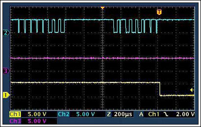
Figure 8. Partial emulation with DS2406, output activation.
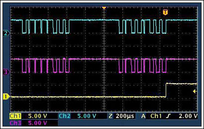
Figure 9. Partial emulation with DS2406, output deactivation.
DS2413 Addressable Switch
The circuit of Figure 7 has also been tested using the DS2413 addressable switch. The IN pin of the analog switch was connected to PIO-A of the DS2413. PIO-B was used as a control output to turn on an LED. The PIOs were operated using the PIO Access Write command (code 5Ah). Figure 10 shows the output activation sequence. Visible in the top trace are the PIO Output Data Byte (first true FEh and then inverted 01h), followed by the AAh confirmation byte, and the new PIO Pin status (3Ch). PIO-A (bottom trace), which controls the analog switch, changes right after the inverted PIO Output Data byte. Consequently, the confirmation byte and PIO pin status are passed through to the 1-Wire output (center trace). A reset/PD cycle must be issued to ensure that the slaves on the activated output are synchronizated with the master.
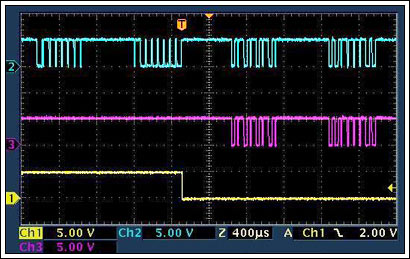
Figure 10. Partial emulation with DS2413, output activation.
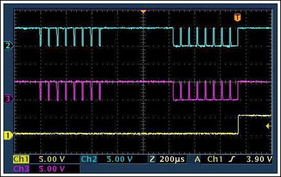
Figure 11. Partial emulation with DS2413, output deactivation.
Figure 11 shows the output deactivation sequence. Visible in the top trace is the PIO Output Data Byte (first true FFh and then inverted 00h). The confirmation byte and the new PIO Pin status (3Ch) are not included in the picture. The PIO-A (bottom trace), which controls the analog switch, changes right after the inverted PIO Output Data byte. The confirmation byte and PIO pin status are not passed through to the 1-Wire output (center trace).
Note that it takes more than 5 minutes after disconnection from the 1-Wire bus for the DS2413 to perform a power-on reset. The DS2406, in contrast, undergoes a power-on reset cycle within 1 minute. The DS2413 has no activity latches and does not support conditional search. Short detection, however, is possible (dotted line).
DS28E04 Addressable Switch
The DS28E04 is a 1-Wire EEPROM with two PIOs. For the PIOs to power up in the nonconduction state, the POL pin needs to be tied to high (5V). The two PIOs are controlled in the same way as with the DS2413. Therefore, Figures 10 and 11 apply here as well. In parasitic power mode, the DS28E04 needs less than 15s of disruption to the 1-Wire bus until it performs a power-on reset. The DS28E04 has activity latches at its PIOs. Therefore, it can support event detection (conditional search) and short detection (dotted line). The activity latches are cleared through the Reset Activity Latches command.
Full Emulation (DS2408 Addressable Switch)
The circuit in Figure 7 shows how to emulate a) one switched 1-Wire output together with the control output, but no event/short detection; and b) one switched 1-Wire output with event/short detection. The limitation comes from the 2-channel addressable switch. For a full emulation one needs five PIO channels (Figure 12).
The full emulation circuit uses two analog switches (U2, U3), which are controlled by PIO ports P1 and P2 of the DS2408 8-channel addressable switch (U1). Ports P2 and P3 connect to the switched 1-Wire outputs. This allows short detection and event sensing. P4 is used to emulate the control output. This leaves P5 to P7 open for other uses. If desired, one could control another analog switch through P5, thus implementing a third 1-Wire output with P6 as short/event sensor. P7, together with P4, could feed into a decoder (not shown) to indicate which of the three 1-Wire outputs is active.
The PIOs of the DS2408 are controlled in the same way as with the DS2413. Therefore, Figures 10 and 11 also apply here. The conditional search of the DS2408 can be programmed to qualify if an event occurred at any of its PIOs. The activity latches are cleared through the Reset Activity Latches command.
In contrast to other addressable switches, the DS2408 needs an external reset signal (U4) to ensure that the PIOs power up in the inactive state. In parasitic power mode, a disruption of less than 5s on the 1-Wire bus causes the DS2408 to perform a power-on reset.
ESD Protection
The DS2409 has a built-in ESD protection on the 1-Wire input and on both 1-Wire outputs. Therefore, additional ESD protection is not necessary. The same is true for the 1-Wire inputs of the 1-Wire addressable switches, but not for their PIO pins. Most analog switches have very limited ESD protection on their pins. Additional protection is highly recommended, in particular for nodes with connectors to the incoming and outgoing 1-Wire networks. Therefore, when selecting ESD protection chips, look for those that add very little capacitance to the bus, such as products from the MAX3202E/MAX3203E/MAX3204E or MAX3207E/MAX3208E series.
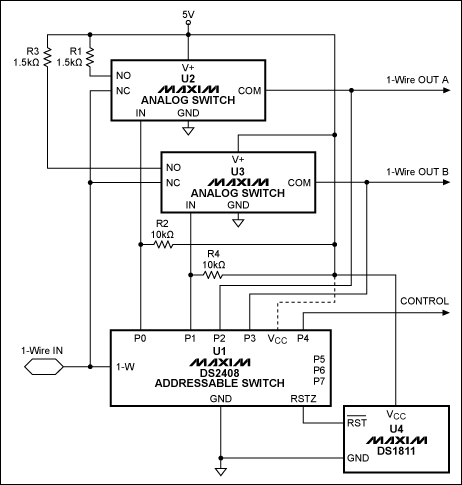
Figure 12. Full DS2409 emulation circuit.
Summary
The DS2409 is a very efficient device to create and operate a large 1-Wire network from a single master. Other key applications are smart access points for access control and dual-master 1-Wire networks. The DS2409 is being phased out, which will cause some hardships for companies that have been relying on the device. This application note shows that there are alternate ways to support the same applications without the DS2409.
1-Wire is a registered trademark of Maxim Integrated Products, Inc.
iButton is a registered trademark of Maxim Integrated Products, Inc.
MicroLAN is a trademark of Maxim Integrated Products, Inc.
 电子发烧友App









评论