DELL最近宣布首款采用ARM架构的服务器--“Copper”,这是自HP推出ARM架构的服务器之后又一家强有力的生产商
2012-05-30 09:39:39 1612
1612 
BOARD LEVEL HEAT SINK
2023-03-23 05:05:36
散热片 TO-220 铜 1.0W @ 20°C 插件板级,垂直
2024-03-14 20:37:16
HEATSINKCOPPERTO-220W/TABS
2023-03-23 05:05:33
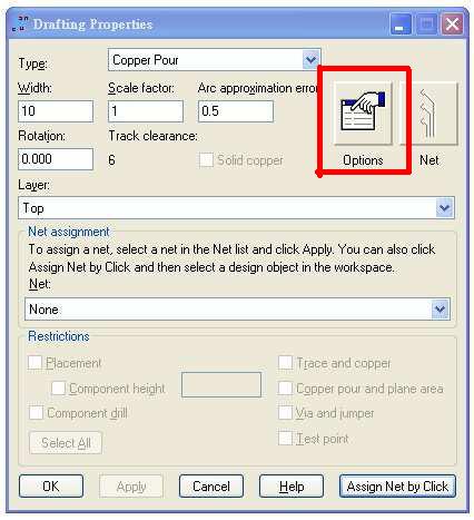
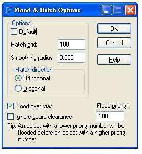
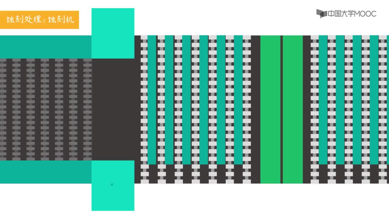
flood比较正确的说法应该叫灌铜,是指对用(Copper Pour)画幅出来的闭合区域根据设定规则进行铺铜的一个动作。而铺铜是指用Copper手动画铜皮。而对于Flood和Hatch的区别,在帮
2011-12-13 14:27:03
of network, copper and fiber testing tools all bundled together in a Professional Test Kit at a discounted price.
2019-09-03 13:48:24
addresses the parameters for testing grounding connections on aluminum, copper, steel, copper
2008-08-11 23:54:29
of network, copper and fiber testing tools all bundled together in a Professional Test Kit.
2019-07-05 10:09:39
values of following Component Definition properties found on R19 and R18 for part "R"
2017-12-17 17:45:05
; 右键,选择Properties…Obstacle type:障碍物类型Anti-copper area:反铺铜Board Outline:边框Comp group keepin:Group组器件的放置
2008-05-12 22:12:23
PADS Layout 9.3 移动Copper时偶尔可以看见Copper的外型边框,但是看不见里面的铜皮,我试着查找了许多设置都无法解决,我要怎么处理这个问题。
2023-09-16 10:51:47
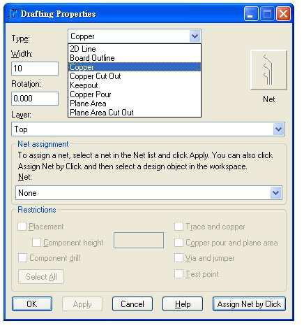
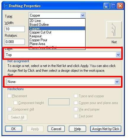
PADS :Copper Properties中敷铜方法和属性有哪些PADS有哪些敷铜方法呢
2015-01-04 10:49:56
本帖最后由 fred999 于 2013-3-14 22:55 编辑
1. 使用 PADS9.5 覆铜, Design Rules 里 Default rules 已经设置 Copper 与其
2013-03-14 22:24:31
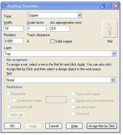
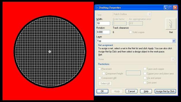
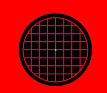
。2-1.如何控制所铺铜皮为网格或实心?1.Opttions->Grids->Hatch grid中可以设置Copper值,2.选中铜皮,右键->Properties,在Drafting
2013-02-18 18:14:36
only create Copper and Copper Pour areas on the layer.· CAM Plane— Sets the entire layer
2015-01-27 13:43:14
要教唆大家剑走偏锋?打工是不可能打工的了?其实老wu这里说的盗铜,指的是 Copper Thieving啦。
2021-02-25 06:15:05
1、 层压板:laminate2、 基材:base material3、 增强板材:stiffener material4、 铜箔面:copper-clad surface5、 去铜箔面:foil
2012-08-01 17:51:21
】:Flood灌铜,也产生这样的效果。无模命令po显示Copper pour区边框并选中后,右键->roperties,在Drafting Properties中有Width设置值;在Options
2019-02-15 02:39:59
KITSFP+COPPER8.5GBS8M30AWG
2023-03-30 11:43:32
KITSFP+COPPER8.5GBS15M24AWG
2023-03-30 11:43:25
KITSFP+COPPER10GBPS12N24AWG
2023-03-30 11:43:25
KITSFP+COPPER10GBPS7M30AWG
2023-03-30 11:43:32
ccs里project properties是白色的,点不了
2019-08-23 10:52:50
pads layout里copper pour cut out后在里面再铺一块铜皮灌不进铜求助,该如何设置?
2016-03-01 10:39:53
pads铺铜时copper pour边框大时,不能自动删除孤铜!稍微小点的时候能自动删除孤铜,这是为啥呀呀呀呀.....求助!!!
2012-08-11 09:26:07
Hello Hugo,如果协议有标头中的字节数(即数据包大小指示符),那么假设标题总是固定的字节数,那么首先要对标准数字进行二进制读取。头文件的字节然后解析并计算要读取多少字节,然后对该字节数进行二进制读取和Voila'....我们有一个更复杂的协议来处理这里,DF1.Which没有数据包大小指示符,数据包以转义序列开始,以转义序列结束,因此我们必须一次读取一个字节,并且必须分析每个字节(真正的皇室痛苦 - 但PC今天非常快,所以它不是很明显).Regards .... Rob“Hugo Renkema”于06/05/2003 06:33:38 AMPlease回应“Hugo Renkema”To:“VEE vrf”cc:Subject:[vrf] No read terminator符号RS232 communicationHello everyone,这是我在vrf邮件列表中的第一篇文章。如果没有,我希望我的问题得到很好解释;随时可以询问更多信息。我正在使用HP-VEE 6.01通过RS232与设备通信。通信发生的协议没有EOL符号。 message-bodydoes包含NoB(字节数),表示themessage的长度。当从PC向此设备发送命令时,这在HP-VEE中不是问题。设备发回响应时会发生此问题。此响应也没有EOL符号。因此,HP-VEE不知道何时收到总消息。这导致响应显示在BUS I / O MONITOR中,但在DIRECT IO组件中没有读命令。这是由于事实上,必须填写的读取终止符对于每个单独的响应是不同的。问题很简单(并且希望答案也是如此)。如何读取从COM端口获取的astring,当主题的最后一个字节未知时使用HP-VEE。事先谢谢,Hugo RenkemaEmail:tkip@gastec.nl---您目前订阅的是vrf:ramarquardt @ ra.rockwell.com要订阅,请发送一封空白电子邮件至“join-vrf@it.lists.it.agilent.com”。要取消订阅,请发送一封空白电子邮件至“leave-vrf@it.lists.it.agilent.com”。要将邮件发送到此邮件列表,请发送电子邮件至“vrf@it.lists.it.agilent.com”。如果您需要有关邮件列表的帮助,请发送邮件至“owner-vrf@it.lists.it.agilent.com” .---您目前订阅了vrf:r***@soco.agilent.com要订阅,请发送一封空白电子邮件至“join-vrf@it.lists.it.agilent.com”。要取消订阅,请发送空白电子邮件至“离开” -vrf@it.lists.it.agilent.com“。要发送邮件到此邮件列表,请发送电子邮件至”vrf@it.lists.it.agilent.com“。如果您需要有关邮件列表的帮助,请发送邮件至“owner-vrf@it.lists.it.agilent.com”。 以上来自于谷歌翻译 以下为原文Hello Hugo,If the protocol has, as you say, the number of bytes in the header(viz A packet size indicator),then assuming the header is always a fixed number of bytes,you first do a binary read of the standard number of bytesfor the header then parse that and compute how many morebytes to read, then do a binary read for that number of bytesand Voila'....We have a bit more complex protocol to deal with here, DF1.Which has no packet size indicator, the packet starts withan escape sequence and ends with an escape sequence,so we have to read it one byte at a time and have to analyzeeach byte as it comes in (a real royal pain - but the PC'sare pretty fast today so it is not very noticeable).Regards....Rob"Hugo Renkema" on 06/05/2003 06:33:38 AMPlease respond to "Hugo Renkema" To: "VEE vrf" cc:Subject: [vrf] No read terminator symbol RS232 communicationHello everyone,This is my first post in the vrf Mailing List. I hope my problem isexplained well, if not; feel free to ask for more information.I am using HP-VEE 6.01 to communicate with a device via RS232. The protocolby which the communication takes place has no EOL-symbol. The message-bodydoes contain a NoB (Number of Bytes) which indicates the length of themessage.When sending commands from PC to this device, this is not a problem inHP-VEE. The problem occurs when the device sends back a response. Thisresponse also has no EOL-symbol. Therefore HP-VEE doesn't know when thetotal message is received.This results in the fact that the response is shown in the BUS I/O MONITOR,but not available with a read-command in a DIRECT IO component.This is due to the fact that the read terminator, which must be filled in,is different for every single response.The question is simple (and hopefully the answer too). How to read astring, obtained from a COM-port, using HP-VEE when the last byte of themessage is unknown.Thanks in advance,Hugo RenkemaEmail: tkip@gastec.nl---You are currently subscribed to vrf as: ramarquardt@ra.rockwell.comTo subscribe send a blank email to "join-vrf@it.lists.it.agilent.com".To unsubscribe send a blank email to "leave-vrf@it.lists.it.agilent.com".To send messages to this mailing list,email"vrf@it.lists.it.agilent.com".If you need help with the mailing list send a message to"owner-vrf@it.lists.it.agilent.com".---You are currently subscribed to vrf as: r***@soco.agilent.comTo subscribe send a blank email to "join-vrf@it.lists.it.agilent.com".To unsubscribe send a blank email to "leave-vrf@it.lists.it.agilent.com".To send messages to this mailing list,email "vrf@it.lists.it.agilent.com".If you need help with the mailing list send a message to "owner-vrf@it.lists.it.agilent.com".
2018-09-05 09:50:32
vscode的STM32c_cpp_properties的配置{ "configurations": [{"name": "Win32"
2021-08-23 07:27:55
在PADS中为 copper 形状和 trace 创建精确的外框和拐角功能增强了。显示和打印 copper 和 trace的方法限制了精度,因为 traces 和 copper 外框是以相等于
2019-07-25 04:00:00
`在Pads Layout中1、 新建一个Decal,放一个 半径40mil(1mm)的圆盘(Top层)2、 在其周围放置一个半径120mil(1.5mm)的Copper Cut Out(Top层
2015-01-08 10:38:06
谁可以告诉我为什么这个PADS的PCB文件在底面不能进行COPPER POUR?
2013-11-12 10:15:19
在建库是使用copper和copper cutout组合了个图形,但是导入CST仿真时这块全都短路在一起了。详情请见图,求高手指导。PADS库:大长方形是copper,两边圆形和小长方形是copper cutout。
2016-09-18 21:36:57
220mm,宽440mm,厚40mm总长度不限Raw materials for copper foil soft connection: international use
2018-06-08 10:09:53
为什么在ad18 properties属性对话框中不能输入中文呢?输入的中文都变成了一个个方框。
2020-07-19 17:24:59
, product characteristics, copper braided line uses the high quality round copper wire ( 0.06,0.08
2019-02-25 11:07:34
`管脚连接了地线,copper pour铺地就无法连接了?COPPER POUR区域也定义为GND网络了。打样回来的板子也没有问题,不知道为什么点击地线网络,铺地没有链接到一起?`
2011-06-22 11:20:36
Warnings------------------------------------------------------------------LCD2Shorted Copper
2017-02-17 17:14:28
想通过覆铜走大电流,直接用Copper来画,画好后设置Drafting Properties,可是在这块铜皮上好像添加不了过孔......是不是分块覆铜不是这样操作的?望高手指点指点
2013-10-25 16:54:47
AD18属性对话框properties顶部的搜索框的功能?使用方法?
2019-04-01 07:35:26
最近听说一个新名词叫 均流块(Copper Thieving)。请问orcad如何设置Copper Thieving参数?
2022-07-21 08:40:40
做的灯板圆形的,需要20并5串,有一圈的LED是40个需要copper一半,用的copperpour+copperpour cutout--combine后形成整个圆环,需要解决问题我只需要一半的圆环怎么解决,有知道吗?
2019-05-05 09:30:58
本帖最后由 一只耳朵怪 于 2018-6-11 15:09 编辑
如果想要监视变量Unit32 pluse_number ,每1ms加1,Graph Properties的设置应该怎么设定
2018-06-11 00:44:06
, and the possibility of having interactive TV services such as On-Line-Banking and Movies-0n-Demand. These requirements are pushing the limits of the copper...
2019-06-12 10:30:41
This Application Note presents VCSEL laser driver design using a .13um CMOS process with 8 copper metalization layers.
2019-06-14 15:01:51
。Material: copper bu***ar, copper bu***ar or copper confluence row, ground copper row, is made of copper
2018-06-08 10:00:55
EN71-1:2005 Part1标准Safety of toys —Part 1: Mechanical and physical properties
2009-08-14 22:13:53 27
27 The first technique for maximum heat sinking is to use a heavylayer of copper. 2 oz. copper
2009-09-02 10:46:3129 CAN Copper to Fiber ConverterModel CANFBModel CANFB isolates and protects your CAN (Control Area
2009-11-27 11:06:1134 microscopy (AFM) to image the mechanical properties of soft materials. Tribological and viscoelastic properties have bee
2010-08-03 12:51:026 IntroductionMeasuring electromagnetic properties of materials can provide insight into applications
2010-08-09 10:37:584 to Copper Media Converter. Such a device will take the copper signal and convert it to an optical signal to be transported over a fiber link. A pair
2009-04-20 08:58:021169 
) 5、单面覆铜箔层压板:single-sided copper-clad laminate 6 copper-clad
2009-04-20 09:06:132763 to Copper Media Converter. Such a device will take the copper signal and convert it to an optical signal to be transported over a fiber link. A pair
2009-04-29 09:33:551008 
网络内容(Net Properties)字段
新增 “网络内容” 在Constraint Manager 当中, 将取代传统设定properties 的方式, 您可直接在此输入所需
2009-09-06 11:24:511352 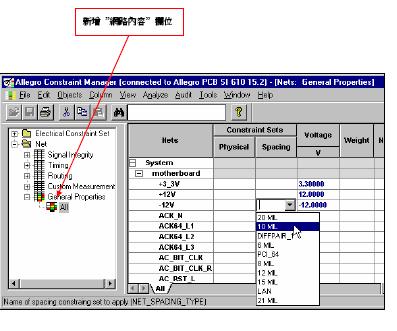
Trace thickness
The thickness of a trace is usually .0014 per ounce of copper.
Our standard material is 1/2 ounce copper that is plated up ano
2009-12-29 09:20:351379 What is the copper plating thickness?
Solution 1 ounce copper is 1.3 to 2.0 Mil thick2 ounce copper is 2.6 to 4.0 Mil thick
2009-12-29 09:26:26852 什么是CDDI (Copper Distributed Data Interface)
英文缩写: CDDI (Copper Distributed Data Interface)
中文译名: 铜线分布式数据接口
2010-02-22 10:55:19627 PADS铜的属性设置及铺铜的方法
在 PCB 设计上,铺铜是相当必要的动作,而 PADS 提供了三种铺铜方法,可让使用者在Copper Properties 中方便的切换,以下就为各位介绍三种
2010-03-21 17:56:5052168 有时修改一个做好板子,或因为某种原因要删除分配好网络的铺铜copper pour,如果直接点击删除,对于一个稍微复杂的PCB,要等好久,这不是我们期望的,采用如下方法或许可以帮你节约
2011-11-11 11:54:4515731 The material of lead frame is phosphor bronze alloy and the die bonded surface is plated by copper and silver. The minimum thickness of plating is 3.0㎛.
2012-02-15 10:02:4818 2012年6月4日北京讯——全球整合式芯片解决方案的领导厂商美满电子科技(Marvell,NASDAQ:MRVL)今天宣布Dell最新推出的“Copper” ARM架构服务器采用了Marvell公司ARMADA® XP芯片。凭借对
2012-06-05 09:13:371012 在PADS中为 copper 形状和 trace 创建精确的外框和拐角功能增强了。
2012-06-26 15:19:365624 2012-09-28 22:02:010 AP0101 Polygon Pours and Copper Regions,很好的学习资料
2016-01-14 15:35:050 Features • miniBLOC package - Electrically isolated copper base - Low coupling capacitance
2017-09-21 10:22:268 Features • International standard package • Direct copper bonded Al2O3-ceramic with copper base
2017-09-21 10:46:026 Features ● International standard package ● Direct copper bonded Al2 O3 -ceramic with copper base
2017-09-21 12:10:1112 本文档内容介绍了基于java不重启服务动态加载properties文件及源代码,供参考
2018-03-12 16:08:340 PADSTACK:就是一组PAD的总称。Copper pad:在布线层(routing layer)。
2018-04-03 10:53:3521638 android.permission.ACCESS_CHECKIN_PROPERTIES允许读写访问”properties”表在checkin数据库中,改值可以修改上传( Allows
2018-05-05 14:21:006374 美国Copper Mountain Technologies(CMT)是业内首家设计创新型USB式的高性能矢网。
2018-06-20 10:52:364537 Flammability VW-1, FT-1, -F- 3. Excellent abrasion resistance and mechanical strength. Copper braid / wire
2018-06-29 15:49:55263 近日,据外媒报道,Facebook正在与英特尔合作以改进其即将推出的Copper Lake架构处理器。
2019-03-18 11:37:55490 Copper foil(铜箔):一种阴质性电解材料,沉淀于线路板基底层上的一层薄的、连续的金属箔,它作为PCB的导电体。
2019-10-28 16:52:006245 铜是一种较贵重的金属,是一种过渡元素,英文copper,化学符号Cu,原子序数29。
2020-06-03 09:18:421746 隐藏如图所示 在properties 界面下面guide manager 下面的enable取消使能相应的即可
2020-10-19 10:29:47933 
AS8510_EvalSW_CShunt_v0-0-8-0.exe Software for Reference Design (Copper Shunt)
2021-01-21 07:17:0725 Copper Mini Shunt
2021-02-23 08:10:169 电子发烧友网为你提供PCB Copper Thieving有什么用?资料下载的电子资料下载,更有其他相关的电路图、源代码、课件教程、中文资料、英文资料、参考设计、用户指南、解决方案等资料,希望可以帮助到广大的电子工程师们。
2021-04-04 08:54:545 修改选错型号右键工程–>properties
2021-12-16 16:54:030 基板材料覆铜箔层压板(Copper Clad Laminaters,CLL),简称覆铜箔层或覆铜板,是制造PCB的基板材料。
2022-10-13 11:16:582160 按照覆铜板的机械刚性可以划分为:刚性覆铜板(Rigid Copper Clad Laminate)和挠性覆铜板(Flexible CopperClad Laminate) 。
2022-12-26 15:39:151679 覆铜陶瓷基板(Direct Plating Copper, DPC)工艺:是一种用于制备高密度电子封装材料的工艺方法。
2023-06-06 15:31:51700 陶瓷基板DPC(Direct Plating Copper)工艺和DBC(Direct Bond Copper)工艺是两种常用的陶瓷基板制作工艺。尽管它们都是用于制作陶瓷基板的方法,但它们之间存在一些重要的区别,导致DPC工艺比DBC工艺更贵。
2023-07-28 10:57:27928 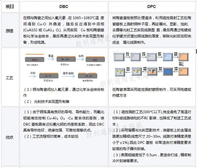
、100BASE-TX和10BASE-T标准化的以太网mac层部分。88E1512-A0-NNP2C000兼容RGMII(适用于相互连接的减少管脚数的GMII)到带自动化介质检测的Copper/Fiber/SGMII、RGMII到Copper、RGMII-SGMII/Fiber和SGMII-Copper。
2023-08-09 14:00:48968
 电子发烧友App


 工商网监
工商网监
评论