Abstract: As integrated circuits (ICs) speed up, the rise/fall times of most pulse and function generators (5ns typical) become inadequate for measuring time intervals below 20ns. You can overcome this limitation with analog switches or advanced CMOS logic gates, which create faster digital edges. The turn-on/ turn-off times for these switches produce very fast rise/fall times. A single-pole double-throw (SPDT) switch can create pulses whose high and low levels are programmable.
Lilliputian dimensions associated with the sub-micron geometries of most digital and many analog processes result in much faster circuit operation. As ICs speed up, the rise/fall times of most pulse and function generators (5ns typical) become inadequate for measuring time intervals below 20ns. You can overcome this limitation with analog comparators or advanced CMOS logic gates, which create faster digital edges. Their rise/fall times are fast enough, but the signal levels include ground and VCC only.
The sub-micron processes used in high-speed digital circuits have been applied to analog switches as well, so the turn-on/ turn-off times for these switches also produce very fast rise/fall times. What's more, a single-pole double-throw (SPDT) switch can create pulses whose high and low levels are programmable.
A feature of the analog switch that hinders its use as a pulse generator is the intrinsic built-in delay (break-before-make time) that guarantees a SPDT switch does not short the two switched terminals together during a transition. Unfortunately, this delay and the switches' finite turn-on time also extends the rise and fall times. You can avoid this effect by adding a dynamic pull-up and pull-down to the circuit (Figure 1). A sufficiently low pull-up/pull-down impedance can drastically improve the corresponding rise and fall times.

Figure 1. The dynamic pullup and pulldown provided by analog switches at the output of this pulse generator ensures fast rise/fall times.
The input clock signal (Φ1) controls a SPDT analog switch (U1) configured as the pull-up/pull-down driver. Φ1 is also sent through a high-speed CMOS inverter (U3) to create a delayed clock signal (Φ2). The delayed clock drives a SPDT analog switch (U2) configured as the output driver.
Consider the steady state condition in which Φ1 is low and Φ2 is high. U1's COM pin and U2's COM pin connect to V_LOW, and a rising edge on Φ1 causes U1 to pull the output signal high. Because the series resistor R1 is large with respect to the MAX4644 on-resistance (47Ω vs. 2.5Ω typical), the immediate affect on output voltage is minimal. Once Φ1 propagates through the inverter string, however, the falling edge of Φ2 causes U2 to transition from VIN(LOW) to VIN(HIGH). The presence of a low-impedance pull up (R1) provides drive for the signal transition, and is closely followed by the closing of U2.
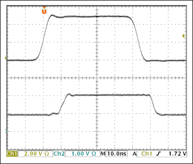
The input signal is 5V logic, and the output swings from 1V to 2V (Figure 2). You can set VIN(LOW) and VIN(HIGH) to any levels within the supply range for U1 and U2. Note that quiescent current for the circuit is essentially zero, with brief peaks only during the output transitions. Rise/fall times at the output are about 4ns, and the output impedance is 2.5Ω.

Figure 2. Figure 1's input (lower trace) and output (upper trace) illustrates fast output transitions and settable output levels.
A similar version of this article appeared in the May 3, 2001 issue of EDN magazine.
Lilliputian dimensions associated with the sub-micron geometries of most digital and many analog processes result in much faster circuit operation. As ICs speed up, the rise/fall times of most pulse and function generators (5ns typical) become inadequate for measuring time intervals below 20ns. You can overcome this limitation with analog comparators or advanced CMOS logic gates, which create faster digital edges. Their rise/fall times are fast enough, but the signal levels include ground and VCC only.
The sub-micron processes used in high-speed digital circuits have been applied to analog switches as well, so the turn-on/ turn-off times for these switches also produce very fast rise/fall times. What's more, a single-pole double-throw (SPDT) switch can create pulses whose high and low levels are programmable.
A feature of the analog switch that hinders its use as a pulse generator is the intrinsic built-in delay (break-before-make time) that guarantees a SPDT switch does not short the two switched terminals together during a transition. Unfortunately, this delay and the switches' finite turn-on time also extends the rise and fall times. You can avoid this effect by adding a dynamic pull-up and pull-down to the circuit (Figure 1). A sufficiently low pull-up/pull-down impedance can drastically improve the corresponding rise and fall times.

Figure 1. The dynamic pullup and pulldown provided by analog switches at the output of this pulse generator ensures fast rise/fall times.
The input clock signal (Φ1) controls a SPDT analog switch (U1) configured as the pull-up/pull-down driver. Φ1 is also sent through a high-speed CMOS inverter (U3) to create a delayed clock signal (Φ2). The delayed clock drives a SPDT analog switch (U2) configured as the output driver.
Consider the steady state condition in which Φ1 is low and Φ2 is high. U1's COM pin and U2's COM pin connect to V_LOW, and a rising edge on Φ1 causes U1 to pull the output signal high. Because the series resistor R1 is large with respect to the MAX4644 on-resistance (47Ω vs. 2.5Ω typical), the immediate affect on output voltage is minimal. Once Φ1 propagates through the inverter string, however, the falling edge of Φ2 causes U2 to transition from VIN(LOW) to VIN(HIGH). The presence of a low-impedance pull up (R1) provides drive for the signal transition, and is closely followed by the closing of U2.
The input signal is 5V logic, and the output swings from 1V to 2V (Figure 2). You can set VIN(LOW) and VIN(HIGH) to any levels within the supply range for U1 and U2. Note that quiescent current for the circuit is essentially zero, with brief peaks only during the output transitions. Rise/fall times at the output are about 4ns, and the output impedance is 2.5Ω.

Figure 2. Figure 1's input (lower trace) and output (upper trace) illustrates fast output transitions and settable output levels.
A similar version of this article appeared in the May 3, 2001 issue of EDN magazine.
 电子发烧友App













评论