Abstract: The following application note discusses the advantages of using the DS1632 PC Power Fail and Reset Controller to consolidate various power management functions into one device vs. using discreet components. The DS1632 performs clock signal generation, reset generation, power-fail signal generation and generation of a low battery signal.
Pin Configuration
Pin Description
The DS1632 has been specifically designed to consolidate various power management functions into one device. The DS1632 can perform four system functions:

Figure 1. Oscillator.
The DS1632's oscillator requires only the 32.768kHz crystal input. The DS1632's oscillator is tuned to accept a 6pF load and to provide an accuracy of ±2 minutes/ month when used with either the Daiwa DT26S, the Seiko DS-VT-200 or an equivalent crystal.
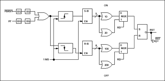
Figure 2. Reset generation.
To provide the same functions as the DS1632 reset generator system, a designer would have to use a 5-bit counter, an 8-bit counter, 2-3 nand gates, an octal latch, an octal inverter, a single inverter, and a 1ms clock signal to the circuit. The DS1632 replaces these discrete components, providing piece part count reduction which conserves circuit board space.
The DS1632 accepts triggers for resets from:
The DS1632 not only generates active-low PF and PF signals for an out of tolerance VCCI, but also switches between VCCI and an external supply to provide an uninterrupted VCCO, regardless of the status of VCCI. The discrete circuitry required to duplicate these functions is illustrated in Figures 3 and 4.

Figure 3. Power fail signal generation.

Figure 4. External battery supply switching.
Duplicating the DS1632's power fail and switching functions would require constructing or buying a band gap voltage reference, 3 resistors, 1 mux, 2 comparators, and 2 P-channel mosfets, and an inverter. The solution implemented discretely would also require more operating current than the condensed functionality provided by the DS1632.

Figure 5. Backup battery monitoring.
From the diagram, duplicating the battery fail detection system would require the use of two resistors, one op amp, one comparator, an inverter, and an accurate voltage reference, such as that provided by a band gap reference, for comparison. The DS1632 produces the band gap voltage reference internally, as well as eliminating the need for the resistors and other external components.
The DS1632 provides these functions in low pin count 16 pin DIP or SOIC package. In addition, the DS1632 solution is built from a very low power CMOS process, giving added reliability and lifetime to battery operated and battery backed up systems. The DS1632 also provides the benefit of a stable clock oscillator which aids in accurate timekeeping for the chipset resident real time clock. All things considered, the DS1632 provides the ideal answer for PC chipset battery operated and battery backed up applications.
* Discrete materials costs are estimates. Actual costs may differ.
** DS1632 pricing listed is for an order quantity of 5,000 pieces.

Figure 6. Consolidated solution for DS1632.

VCCO from the DS1632 connects directly to the 82360SL, RTC VCC, input pin 177, to provide an uninterrupted power supply to the 82360's real time clock, regardless of the status of VCC.
OSCOUT from the DS1632 connects directly to the 82360SL, RTC X1 input, providing the 82360SL with a 32.768kHz square wave input.
Active-low RESET from the DS1632 connects directly to the RC# input, pin 58, of the 82360SL, providing a signal which triggers the 82360SL to produce a reset on its CPU RESET output pin.
LB from the DS1632 connects directly to the 82360SL through any of the IRQ pins (interrupt request). The interrupt request service routine for that interrupt must be configured to perform a function acknowledging the low battery status of the 3V cell connected to the DS1632.
RESET from the 1632 connects directly to the 386SL processor input, CPU RESET, pin 2, providing an active high signal to reset the processor. This signal can be provided alternatively through the 82360SL's CPU RESET output, triggered by the active-low RESET signal from the DS1632.
Active-low PF from the DS1632 connects directly to the PWR GOOD input of the 386SL, pin 18. When active-low PF from the DS1632 is high, PWR GOOD allows the 386SL to operate normally. When active-low PF becomes active low, PWR GOOD going low on the 386SL causes the processor to reset its core, internal state machines, and configuration registers.
The DS1632 is designed to provide its interrupt monitoring signals in complemented sets so that the DS1632 can be connected to any microprocessor or chip set without having to invert the outputs.
The diagram below, "Chips Technologies/Siemens 82C206 Connections", shows the DS1632 connecting to the popular AT bus chip. In this configuration, the DS1632 provides: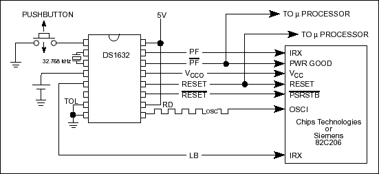
Active-low PF from the DS1632 connects directly to pin 14, PWR GOOD, of the 82C206. When active-low PF becomes active low, the 82C206's address, data, strobe, and R/W pins are disconnected from the microprocessor.
PF can be connected to one of the 82C206's interrupt request pins (IRQ pins) to act as a warning that VCC is out of tolerance or sent to the µp as an interrupt.
VCCO from the DS1632 connects directly to the 82C206's VCC pin. VCCO from the DS1632 can provide for the 82C206's normal operating voltage and current requirements with VCC in tolerance and for sustaining the RTC functions of the 82C206 from its 3 volt power source, VBAT, when VCC is in less than the attached backup battery.
RESET from the DS1632 connects directly to the 82C206 RESET input pin, which resets the 82C206's DMA control registers and interrupt controllers.
RESET from the DS1632 connects to the active-low PSRSTB input of the 82C206. This reset input is primarily a "power on reset" input for the 82C206, but can also act as an externally triggered reset input.
OSCOUT from the DS1632 provides the 32.768kHz oscillator input to the 82C206 through the OSC1 input on the 82C206.
LB from the DS1632 connects directly to an interrupt request line on the 82C206. LB from the DS1632 indicates that the lithium backup cell has fallen out of tolerance.

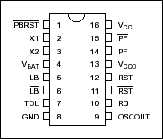
Pin Configuration

Pin Description
| PIN NAME | DESCRIPTION |
| ACTIVE-LOW PBRST | PUSHBUTTON RESET INPUT |
| X1, X2 | CRYSTAL INPUTS |
| VBAT | BATTERY INPUT |
| LB, ACTIVE-LOW LB | LOW BATTERY OUTPUTS |
| RST, ACTIVE-LOW RST | RESET OUTPUTS |
| RD | RESET DURATION |
| TOL | SELECTS 5% OR 10% DETECTION |
| GND | GROUND |
| OSCOUT | OSCILLATOR OUT |
| VCCO | SWITCHED POWER OUT |
| PF, ACTIVE-LOW PF | POWER FAIL OUTPUTS |
| VCC | +5 VOLT POWER IN |
The DS1632 has been specifically designed to consolidate various power management functions into one device. The DS1632 can perform four system functions:
- Clock signal generation (32.768kHz) for a real time clock.
- Reset generation, including external pushbutton reset input.
- Power fail signal generation and transparent switching from VCC to a secondary battery VBAT when VCC is out of tolerance.
- Generation of a low battery signal, indicating the backup battery has fallen out of a minimum acceptable tolerance.
Clock Signal Generation
A system design requiring an accurate timekeeping source or real time clock is best served by using one of the real time clocks offered by Maxim which combine a real time clock, memory, and 10 year non-volatility in the absence of power. However, some designs contain chipsets which provide a real time clock function, without the accuracy or reliability of the Maxim Real Time Clock. For customer designs that must make use of another manufacturer's chipset, the DS1632 provides the highly accurate clock signal generation required to drive a real time clock. A significant part of the accuracy of any digital real time clock is its reliance upon receiving an accurate, consistent clock oscillator input, which the DS1632 provides. The logic required to produce this function discretely is as follows in Figure 1.
Figure 1. Oscillator.
The DS1632's oscillator requires only the 32.768kHz crystal input. The DS1632's oscillator is tuned to accept a 6pF load and to provide an accuracy of ±2 minutes/ month when used with either the Daiwa DT26S, the Seiko DS-VT-200 or an equivalent crystal.
Reset Generation
Generating Reset Signals for a Microprocessor
Reset signal generation for a microprocessor must be triggerable from a variety of sources. Most notably, during a power fail situation, during power up, and externally as a user demanded system reset. The DS1632 provides all three of these functions that would otherwise have to be provided discretely as shown (Figure 2).
Figure 2. Reset generation.
To provide the same functions as the DS1632 reset generator system, a designer would have to use a 5-bit counter, an 8-bit counter, 2-3 nand gates, an octal latch, an octal inverter, a single inverter, and a 1ms clock signal to the circuit. The DS1632 replaces these discrete components, providing piece part count reduction which conserves circuit board space.
The DS1632 accepts triggers for resets from:
- A pushbutton input, high to low, on active-low PBRST.
- VCC coming into tolerance as characterized by a low to high transition on the PF pin which disables reset.
- VCC going out of tolerance as characterized by a high to low transition on the PF pin which triggers reset.
The DS1632 not only generates active-low PF and PF signals for an out of tolerance VCCI, but also switches between VCCI and an external supply to provide an uninterrupted VCCO, regardless of the status of VCCI. The discrete circuitry required to duplicate these functions is illustrated in Figures 3 and 4.

Figure 3. Power fail signal generation.

Figure 4. External battery supply switching.
Duplicating the DS1632's power fail and switching functions would require constructing or buying a band gap voltage reference, 3 resistors, 1 mux, 2 comparators, and 2 P-channel mosfets, and an inverter. The solution implemented discretely would also require more operating current than the condensed functionality provided by the DS1632.
Generation of Low Battery Signal
The DS1632 provides early warning notification that the backup power source is falling out of tolerance and should be replaced. The discrete circuit required to duplicate this functionality is shown in Figure 5.
Figure 5. Backup battery monitoring.
From the diagram, duplicating the battery fail detection system would require the use of two resistors, one op amp, one comparator, an inverter, and an accurate voltage reference, such as that provided by a band gap reference, for comparison. The DS1632 produces the band gap voltage reference internally, as well as eliminating the need for the resistors and other external components.
A System Solution
All four functions of the DS1632 implemented discretely would consume a significant amount of circuit board space with a high piece part count which would drive up costs.The DS1632 provides these functions in low pin count 16 pin DIP or SOIC package. In addition, the DS1632 solution is built from a very low power CMOS process, giving added reliability and lifetime to battery operated and battery backed up systems. The DS1632 also provides the benefit of a stable clock oscillator which aids in accurate timekeeping for the chipset resident real time clock. All things considered, the DS1632 provides the ideal answer for PC chipset battery operated and battery backed up applications.
| DISCRETE SYSTEM BILL OF MATERIALS | EST. COST |
| 32.768KHZ CLOCK OSCILLATOR | $1.50 |
| 5-BIT COUNTER | $ .20 |
| 8-BIT COUNTER | $ .20 |
| LS04 (4 NAND GATES) | $ .20 |
| OCTAL LATCH W/INVERTERS | $ .25 |
| 1MS CLOCK SOURCE | $1.00 |
| BAND GAP VOLTAGE REFERENCE | $ .70 |
| 5 CHIP RESISTORS | $ .10 |
| 1 DUAL INPUT MUX | $ .20 |
| 2 DUAL COMPARATORS | $1.00 |
| 2 FETS | $ .20 |
| LS TYPE INVERTER (QUAD) | $ .20 |
| SUB-TOTAL | $5.75 |
| MAXIM SOLUTION | COST |
| DS1632 | $2.10 |
| DAIWA PART DT26S OR SEIKO PART DS-VT-200 |
$ .35 |
| SUB-TOTAL | $2.45 |
** DS1632 pricing listed is for an order quantity of 5,000 pieces.

Figure 6. Consolidated solution for DS1632.
System Applications
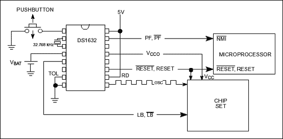
The DS1632 power manager hooks directly to the Intel 386SL superset to provide continuous power to the 82360SL's real time clock, reset signals to both the 82360SL and 386SL, power monitoring signals to the 386SL, oscillator input to the 82360SL's RTC, and backup battery supply monitoring.INTEL 386SL Microprocessor Superset Connections

VCCO from the DS1632 connects directly to the 82360SL, RTC VCC, input pin 177, to provide an uninterrupted power supply to the 82360's real time clock, regardless of the status of VCC.
OSCOUT from the DS1632 connects directly to the 82360SL, RTC X1 input, providing the 82360SL with a 32.768kHz square wave input.
Active-low RESET from the DS1632 connects directly to the RC# input, pin 58, of the 82360SL, providing a signal which triggers the 82360SL to produce a reset on its CPU RESET output pin.
LB from the DS1632 connects directly to the 82360SL through any of the IRQ pins (interrupt request). The interrupt request service routine for that interrupt must be configured to perform a function acknowledging the low battery status of the 3V cell connected to the DS1632.
RESET from the 1632 connects directly to the 386SL processor input, CPU RESET, pin 2, providing an active high signal to reset the processor. This signal can be provided alternatively through the 82360SL's CPU RESET output, triggered by the active-low RESET signal from the DS1632.
Active-low PF from the DS1632 connects directly to the PWR GOOD input of the 386SL, pin 18. When active-low PF from the DS1632 is high, PWR GOOD allows the 386SL to operate normally. When active-low PF becomes active low, PWR GOOD going low on the 386SL causes the processor to reset its core, internal state machines, and configuration registers.
The DS1632 is designed to provide its interrupt monitoring signals in complemented sets so that the DS1632 can be connected to any microprocessor or chip set without having to invert the outputs.
The diagram below, "Chips Technologies/Siemens 82C206 Connections", shows the DS1632 connecting to the popular AT bus chip. In this configuration, the DS1632 provides:
- Out of tolerance VCC and pushbutton reset generation.
- Real time clock oscillator input.
- VCC monitoring and notification of out of tolerance VCC.
- Backup battery monitoring and generation of warning signal, LB, indicating VBAT is out of tolerance.
Chips Technologies/Siemens 82C206 Connections

Active-low PF from the DS1632 connects directly to pin 14, PWR GOOD, of the 82C206. When active-low PF becomes active low, the 82C206's address, data, strobe, and R/W pins are disconnected from the microprocessor.
PF can be connected to one of the 82C206's interrupt request pins (IRQ pins) to act as a warning that VCC is out of tolerance or sent to the µp as an interrupt.
VCCO from the DS1632 connects directly to the 82C206's VCC pin. VCCO from the DS1632 can provide for the 82C206's normal operating voltage and current requirements with VCC in tolerance and for sustaining the RTC functions of the 82C206 from its 3 volt power source, VBAT, when VCC is in less than the attached backup battery.
RESET from the DS1632 connects directly to the 82C206 RESET input pin, which resets the 82C206's DMA control registers and interrupt controllers.
RESET from the DS1632 connects to the active-low PSRSTB input of the 82C206. This reset input is primarily a "power on reset" input for the 82C206, but can also act as an externally triggered reset input.
OSCOUT from the DS1632 provides the 32.768kHz oscillator input to the 82C206 through the OSC1 input on the 82C206.
LB from the DS1632 connects directly to an interrupt request line on the 82C206. LB from the DS1632 indicates that the lithium backup cell has fallen out of tolerance.
 电子发烧友App










评论