The need for ultra-low on-resistance and low switching losses can make notebook MOSFET choice difficult. Nonetheless, MOSFET characteristics dominate DC-DC power conversion efficiency. This is critical for notebook CPUs due out in 1999.
Efficiency is a key issue, not so much because of battery life, but because of heat buildup inside thin notebooks. As batteries improve, upcoming blazing-fast portable systems based on next-generation CPUs will devour energy. Heat will define the upper limit of notebook performance.
Any unnecessary dissipation of 0.5W or more is a problem. As CPUs become more power hungry and supply voltage rails drop, DC-DC converters, needed to convert battery voltage down to next year's low-voltage rails, become increasingly inefficient mainly due to increased conduction losses.
Well, let's say a notebook's CPU is limited to 8W by clock-throttling techniques, and the remainder of the system dissipates about 15W. Assume the battery is removed and the input voltage to the DC-DC converter rises to the maximum an AC adapter is capable of, which is usually about 22V. This voltage (considering tolerance errors in the AC adapter), stacked on the headroom needed to charge a four-cell lithium-ion battery, becomes a key design parameter because of its effect on switching losses.
The best approach is still the conventional buck topology regulator powered directly from a portable's battery. It's simple and exhibits very high efficiency, provided that its MOSFET characteristics are well matched to the required currents and switching frequency. What's needed is a MOSFET family that has a wide spread of Rds(ON) ratings, one that's process-optimized for efficiency at high battery voltages as well as switching frequencies in the 250kHz to 500kHz range.

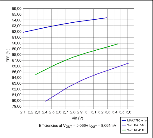
Figure 1. Notebook DC-DC efficiency: 1997 versus 1999.
Although simplified, this spreadsheet analysis was checked against actual breadboard measurements, and the efficiency results are within 1% or 2% of actual measurements. The numbers indicate that we are fairly close to 90% efficiency using today's MOSFETs. (The results assume that some of the latest and greatest MOSFETs, such as the Fairchild Semiconductor FDS6680, International Rectifier IRF7801, and Temic Si4420, will be available in re-sized products scaled appropriately for these supply rails; this is an exercise that has yet to be completed by MOSFET makers.)
The MOSFET parameters for these simulations were generated by taking the specs from the three best MOSFETs available today, creating a hypothetical composite MOSFET with characteristics similar to all three, and then scaling the resistance, the capacitance, and the gate charge parameters linearly with die sizes from 1.5X to 0.125X. Note that the Rds(ON) of the 1.5X devices isn't scaled linearly; this is due to an assumption that package and bond-wire resistance would eat into any gain made by increasing the die size.
MOSFET parameters in 1999 were obtained by assuming that advances in MOSFET processing will yield a 28% improvement in the Rds(ON) x gate charge (Qg) figure of merit, or FOM. Note that this 28% improvement yields only a 3% efficiency gain from today to 1999.
What's more, I2R conduction losses increase as the square of the current, which explains the sudden drop-off in efficiency as output voltages drop below 2V and output power is kept constant. The message is that Rds(ON) in a CPU-supply low-side FET must be minimized. A good target goal is 9m maximum (with Vgs = 5V). MOSFET manufacturers are exploring ways to reduce package parasitic resistances.
Battery voltages of 22V also place thermal stress on high-side MOSFETs due to switching losses, rather than conduction losses. Analyzing switching losses is somewhat of a lost art, because the actual rise and fall times of the switching node are dependent on many variables, including MOSFET source inductance, internal gate resistance, and the effect of gate bond-pad placement on the propagation of the gate-drive signal through the die. Other variables include external gate-driver current capability, Miller capacitance, minority-carrier recombination in the freewheeling diode, and stray inductance induced by circuit board layout.
First-order switching times depend on how fast the gate-driver current can charge the FET's gate-drain capacitance, and that's how the spreadsheet calculations were made. Because of the small duty factor, conduction losses in the high-side FET are less important, so die sizes can be made much smaller than those of high-side FETs. The resulting smaller die size goes a long way toward reducing Miller capacitance and switching losses.
For a given operating frequency, efficiency peaks where switching losses in the high-side FET are equal to conduction losses. If we sweep MOSFET die size from tiny to large, then at the point that Rds(ON) losses are equal to the Miller capacitance induced losses stop. This point represents a local maximum on the efficiency curve. The exact Rds(ON) and Miller capacitance areas of trade-off must obviously be chosen by the MOSFET makers, because each has unique fabrication techniques that result in different threshold and switching characteristics.
One problem with this sizing method is the variable input voltage. Do you choose the minimum battery voltage or the maximum? Let's examine a design methodology.
Next, pick a low-side MOSFET having the lowest possible Rds(ON) that's small enough to come in a reasonable package (such as an SO-8), and won't burn a hole in your budget. Check to ensure that your power-supply controller IC can drive it, and that the gate doesn't get yanked up by the high-side switch turning on (due to parasitic drain-to-gate capacitance), causing cross-conduction problems. Switching losses aren't an issue for the low-side MOSFET, because it is a zero-voltage-switched device when used in the buck topology.
What's needed is a family of MOSFETs, sized for different loads. All of these should be N-channel types because of their superior carrier mobility and smaller die size for a given Rds(ON). N-channel FETs also offer switching-time advantages over their P-channel cousins. For high-voltage applications, P-channel devices offer no reduction in the complexity of gate-drive circuits compared with N-channel devices. Because a 100% duty factor isn't needed, there is no advantage to P-channel devices.
The absolute, maximum Vds breakdown voltage ratings of these transistors can be 25V rather than the 30V that is typically used with this class of MOSFETs. The use of 25V should permit some improvement in die size, thanks to reduced channel lengths; you'll get better Rds(ON) and Miller capacitance, which will improve the FOM.
Gate threshold characteristics should be optimized for 5V gate-drive signals, but the threshold shouldn't be made less than 1V due to the accidental turn-on problem caused by gate-drain capacitance.
Having a MOSFET with a 25V, absolute, maximum drain-source breakdown rating would be ideal. Another item would be asymmetric sizes, based on duty factor. The wish-list devices ideally would include five maximum continuous load current capabilities for 1A, 2A, 3A, 4A, and 8A. The FETs would let you make the right Rds(ON) versus Miller capacitance trade-off, and both high-side and low-side devices would be packaged together as a dual-FET device. About 20 products would be needed, even if packaged as duals.
A spreadsheet analysis indicates that large advances in MOSFET technology are needed to provide even small improvements in DC-DC converter efficiency. Although simplified, this analysis was checked against actual breadboard measurements; efficiency figures were within 1% or 2% of actual results.

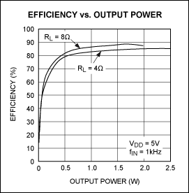
Figure 2. Efficiency versus output voltage.
As supply voltage rails plummet, efficiency typically follows. Loss of efficiency is attributable to increased conduction losses.

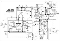
Figure 3. Digitally adjusted CPU supply.
The above example of a digitally adjusted CPU DC-DC supply is based on a MAX1636 controller chip. The circuit is intended for Mobile Pentium II cores. It offers ultra-high DC precision and fast transient response. The components are tailored for low switching and conduction losses.

Figure 4. Conduction losses in a DC-DC converter.
Conduction losses in a typical notebook's DC-DC converter occur in both high- and low-side MOSFETs, the freewheeling diode across the low-side device, sensing resistors, input and output capacitors, and series inductors.
A similar version of this article appeared in the July 1998 issue of Portable Design.
Efficiency is a key issue, not so much because of battery life, but because of heat buildup inside thin notebooks. As batteries improve, upcoming blazing-fast portable systems based on next-generation CPUs will devour energy. Heat will define the upper limit of notebook performance.
Any unnecessary dissipation of 0.5W or more is a problem. As CPUs become more power hungry and supply voltage rails drop, DC-DC converters, needed to convert battery voltage down to next year's low-voltage rails, become increasingly inefficient mainly due to increased conduction losses.
Reaching 90%
What advances are needed to ensure that the average efficiency of a notebook's total DC-DC converter subsystem is at least 90% under worst-case conditions (typically when running 3-D graphics software)?Well, let's say a notebook's CPU is limited to 8W by clock-throttling techniques, and the remainder of the system dissipates about 15W. Assume the battery is removed and the input voltage to the DC-DC converter rises to the maximum an AC adapter is capable of, which is usually about 22V. This voltage (considering tolerance errors in the AC adapter), stacked on the headroom needed to charge a four-cell lithium-ion battery, becomes a key design parameter because of its effect on switching losses.
Choosing the Best Topology
Your design approach is therefore critical. What DC-DC converter topology should you use? What is best in terms of physical partitioning? Should a resonant scheme be used to minimize switching losses? Or should a two-stage DC-DC conversion process be chosen to power the CPU's DC-DC converter from a lower voltage (such as 5V) so that it can be run at very high frequencies and ensure fast transient response?The best approach is still the conventional buck topology regulator powered directly from a portable's battery. It's simple and exhibits very high efficiency, provided that its MOSFET characteristics are well matched to the required currents and switching frequency. What's needed is a MOSFET family that has a wide spread of Rds(ON) ratings, one that's process-optimized for efficiency at high battery voltages as well as switching frequencies in the 250kHz to 500kHz range.
A Comparative Analysis
The accompanying chart shows the output of a poor man's Spice simulator that computed conduction, core, and switching losses separately for 1999 notebook supply rails. You'll notice supply rails of 1.8V and 2.5V. These rails are going to appear in next year's notebooks.
Figure 1. Notebook DC-DC efficiency: 1997 versus 1999.
Although simplified, this spreadsheet analysis was checked against actual breadboard measurements, and the efficiency results are within 1% or 2% of actual measurements. The numbers indicate that we are fairly close to 90% efficiency using today's MOSFETs. (The results assume that some of the latest and greatest MOSFETs, such as the Fairchild Semiconductor FDS6680, International Rectifier IRF7801, and Temic Si4420, will be available in re-sized products scaled appropriately for these supply rails; this is an exercise that has yet to be completed by MOSFET makers.)
The MOSFET parameters for these simulations were generated by taking the specs from the three best MOSFETs available today, creating a hypothetical composite MOSFET with characteristics similar to all three, and then scaling the resistance, the capacitance, and the gate charge parameters linearly with die sizes from 1.5X to 0.125X. Note that the Rds(ON) of the 1.5X devices isn't scaled linearly; this is due to an assumption that package and bond-wire resistance would eat into any gain made by increasing the die size.
MOSFET parameters in 1999 were obtained by assuming that advances in MOSFET processing will yield a 28% improvement in the Rds(ON) x gate charge (Qg) figure of merit, or FOM. Note that this 28% improvement yields only a 3% efficiency gain from today to 1999.
Critical Losses
Switching and conduction losses are both critical. Our worst-case condition of 22V of battery voltage places a tremendous burden on both high- and low-side MOSFETs in a half-H-bridge buck topology. The resulting duty factor of about 7% (at Vout = 1.5V) means the low-side FET is conducting 93% of the time. It must bear the lion's share of conduction losses.What's more, I2R conduction losses increase as the square of the current, which explains the sudden drop-off in efficiency as output voltages drop below 2V and output power is kept constant. The message is that Rds(ON) in a CPU-supply low-side FET must be minimized. A good target goal is 9m maximum (with Vgs = 5V). MOSFET manufacturers are exploring ways to reduce package parasitic resistances.
Battery voltages of 22V also place thermal stress on high-side MOSFETs due to switching losses, rather than conduction losses. Analyzing switching losses is somewhat of a lost art, because the actual rise and fall times of the switching node are dependent on many variables, including MOSFET source inductance, internal gate resistance, and the effect of gate bond-pad placement on the propagation of the gate-drive signal through the die. Other variables include external gate-driver current capability, Miller capacitance, minority-carrier recombination in the freewheeling diode, and stray inductance induced by circuit board layout.
First-order switching times depend on how fast the gate-driver current can charge the FET's gate-drain capacitance, and that's how the spreadsheet calculations were made. Because of the small duty factor, conduction losses in the high-side FET are less important, so die sizes can be made much smaller than those of high-side FETs. The resulting smaller die size goes a long way toward reducing Miller capacitance and switching losses.
Use Asymmetric MOSFETs
The MOSFETs must also be asymmetric. Your high-side FET should be about one-third or one-quarter the size of the low-side MOSFET. This reduces switching losses in the high-side FET and lessens conduction losses in the low-side FET.For a given operating frequency, efficiency peaks where switching losses in the high-side FET are equal to conduction losses. If we sweep MOSFET die size from tiny to large, then at the point that Rds(ON) losses are equal to the Miller capacitance induced losses stop. This point represents a local maximum on the efficiency curve. The exact Rds(ON) and Miller capacitance areas of trade-off must obviously be chosen by the MOSFET makers, because each has unique fabrication techniques that result in different threshold and switching characteristics.
One problem with this sizing method is the variable input voltage. Do you choose the minimum battery voltage or the maximum? Let's examine a design methodology.
Proceed One Step at a Time
Start by picking a high-side MOSFET that has conduction losses equal to the switching losses, at the sweet spot of the battery voltage (16V for a four-cell system). Check to ensure that conduction losses at minimum input voltage don't exceed the FET's package thermal limits, or you will violate your overall thermal budget. Likewise, check to make sure conduction losses plus switching losses at maximum input voltage don't surpass the package ratings, or you'll violate the overall thermal budget.Next, pick a low-side MOSFET having the lowest possible Rds(ON) that's small enough to come in a reasonable package (such as an SO-8), and won't burn a hole in your budget. Check to ensure that your power-supply controller IC can drive it, and that the gate doesn't get yanked up by the high-side switch turning on (due to parasitic drain-to-gate capacitance), causing cross-conduction problems. Switching losses aren't an issue for the low-side MOSFET, because it is a zero-voltage-switched device when used in the buck topology.
N-Channel MOSFETs
So far in this discussion, the spotlight has been on the CPU core supply, as it supports the most demanding system load and has the worst efficiency. But to meet the overall efficiency goal of 90%, your portable design's other supplies must also be improved.What's needed is a family of MOSFETs, sized for different loads. All of these should be N-channel types because of their superior carrier mobility and smaller die size for a given Rds(ON). N-channel FETs also offer switching-time advantages over their P-channel cousins. For high-voltage applications, P-channel devices offer no reduction in the complexity of gate-drive circuits compared with N-channel devices. Because a 100% duty factor isn't needed, there is no advantage to P-channel devices.
The absolute, maximum Vds breakdown voltage ratings of these transistors can be 25V rather than the 30V that is typically used with this class of MOSFETs. The use of 25V should permit some improvement in die size, thanks to reduced channel lengths; you'll get better Rds(ON) and Miller capacitance, which will improve the FOM.
Gate threshold characteristics should be optimized for 5V gate-drive signals, but the threshold shouldn't be made less than 1V due to the accidental turn-on problem caused by gate-drain capacitance.
The Ideal MOSFET
If you could make a wish list of future N-channel MOSFETs for DC-DC converters, here are some things you should include. First, your devices should operate from two input voltage ranges (7V to 18V, and 10V to 22V). These two ranges result from either three- or four-cell lithium-ion cells, respectively.Having a MOSFET with a 25V, absolute, maximum drain-source breakdown rating would be ideal. Another item would be asymmetric sizes, based on duty factor. The wish-list devices ideally would include five maximum continuous load current capabilities for 1A, 2A, 3A, 4A, and 8A. The FETs would let you make the right Rds(ON) versus Miller capacitance trade-off, and both high-side and low-side devices would be packaged together as a dual-FET device. About 20 products would be needed, even if packaged as duals.
A spreadsheet analysis indicates that large advances in MOSFET technology are needed to provide even small improvements in DC-DC converter efficiency. Although simplified, this analysis was checked against actual breadboard measurements; efficiency figures were within 1% or 2% of actual results.

Figure 2. Efficiency versus output voltage.
As supply voltage rails plummet, efficiency typically follows. Loss of efficiency is attributable to increased conduction losses.

Figure 3. Digitally adjusted CPU supply.
The above example of a digitally adjusted CPU DC-DC supply is based on a MAX1636 controller chip. The circuit is intended for Mobile Pentium II cores. It offers ultra-high DC precision and fast transient response. The components are tailored for low switching and conduction losses.

Figure 4. Conduction losses in a DC-DC converter.
Conduction losses in a typical notebook's DC-DC converter occur in both high- and low-side MOSFETs, the freewheeling diode across the low-side device, sensing resistors, input and output capacitors, and series inductors.
A similar version of this article appeared in the July 1998 issue of Portable Design.
 电子发烧友App


评论