The biasing of avalanche photodiodes (APDs), piezoelectric transducers (PZTs), vacuum fluorescent displays (VFDs), and microelectromechanical systems (MEMS) require high-voltage power supplies. This app note presents three topologies (Figures 1a, 1b, and 1c) for generating a high output voltage from a low input voltage. The advantages and disadvantages of each are discussed with focus given to power density and circuit size. The end of the app note presents experimental data to contrast transformer-based and inductor-based solutions.
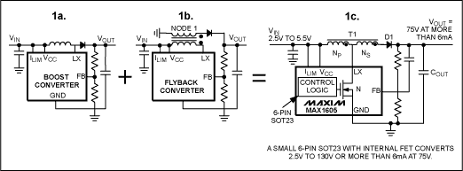
Figure 1a-1c. These high-voltage DC-DC converters in three topologies are used to create high output voltage from low input voltage.
The high-voltage bias required in many APD applications (75V) is derived from a 3V supply. That requirement presents the following challenges:
Figure 2. This 6mm x 8.5mm DC-DC converter converts 2.5V to 75V using the MAX1605. The front and back layout of the circuit is shown.
A transformer provides the following advantages:

where D is the duty cycle. A more analytical proof can be found by using Figure 3. The key to this proof lies in steady-state operation, for which the current must ramp down the same amount that it ramps up:

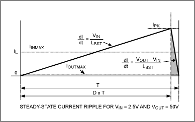
Figure 3. This analysis of the inductor current for the circuit of Figure 1a can be used to determine its duty cycle.
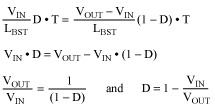
Thus, the final inductor current equals the initial inductor current:

Because they are equal,
The circuit of Figure 1b could be made equivalent to the circuit of Figure 1a by connecting the left side of the transformer's secondary winding to VIN and setting the turns ratio to 1. The secondary-side diode can be reflected to the primary side, making the relationship between a flyback converter and a boost converter easier to perceive.
Turns ratios larger than 1:1 provide leverage by allowing higher output voltage with less extreme duty cycles. Alternatively, node 1 of the transformer can be connected to any power supply, enabling leverage with respect to that supply. Because LX flies up during the off-cycle, an additional voltage step can be obtained by connecting node 1 to LX, as shown in Figure 1c. That connection also helps catch some of the leakage energy that would otherwise be dumped from the transformer's primary side to the MOSFET, producing short, high-voltage spikes at the MOSFET's drain. If the voltage spikes are higher than the MOSFET's voltage tolerance, a snubber circuit will be necessary to dissipate the leakage energy.
LX is shorted to ground in Figure 1b, allowing the primary-side current to ramp up as for an inductor. No current flows through the secondary side of the transformer and the diode is reverse-biased because

Primary-side current must cease when the switch at LX turns off, but the N × I product must remain constant:

where subscript "P" indicates primary side, subscript "S" indicates secondary side, "initial" indicates current at the moment before the MOSFET is switched off, and "final" indicates current at the moment after the MOSFET is switched off.
Because IS_initial = IP_final = 0,

The circuit of Figure 1c is similar, except that IP_final = IS_final, so

To simplify, the turns ratio 'N' is expressed as:

because the secondary side of Figure 1c never acts independently. Though unconventional, this definition for N is more appropriate for Figure 1c.
Figure 4 shows the primary-side current waveform for Figure 1c. For step-up converters whose output is more than twice the input voltage, off-time has a greater effect on the efficiency than on-time. Assume (for a comparable boost converter) that off-time has been minimized by minimizing inductance (LBST), which also minimizes component size to the point that further reduction would lead to undesired efficiency loss. Then, select the Figure 4 transformer's total inductance to be N times as large. Because the primary-side current ramps down from IPK/N instead of IPK, the primary inductance must be N times as large to maintain the same off-time.
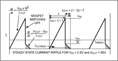
Figure 4. This analysis of the primary-side transformer current for the circuit of Figure 1c can be used to determine its duty cycle.
The primary-side inductance is:

where LTOT is the total inductance of the autotransformer since LBST is N² smaller than LTOT, and LTOT is N times larger than LBST, LP is LBST/N. As a result, the primary side ramps faster than a simple boost converter.

For the steady state, it is clear from Figure 4 that:

where ΔIUP is the upward step in the primary-side current and ΔIDOWN is the downward step. ΔIUP and ΔIDOWN can be calculated as follows:
and

so

Solving for VOUT/VIN yields:

Figures 3 and 4 are both drawn to scale and have the same off-time (set to some optimal minimum). The shaded regions in Figures 3 and 4 represent energy delivered to the load, and the energy per pulse is proportional to the area of those regions. That energy can also be calculated from the expression 1/2 L × I² (note that L in Figure 4 is N times larger, and I is N times smaller). Because the circuit of Figure 1c delivers less energy per pulse, the ripple is N times smaller. Thus, a transformer not only leverages the output voltage up; it also leverages the output ripple down.
The topology of Figure 1c delivers less energy per pulse, but compensates by delivering more pulses, as clearly indicated in Figure 4. Figure 1c requires an N times larger inductance, but the saturation current can be N times smaller because the primary and secondary side see only IPK/N as much current simultaneously. With an ISAT smaller by a factor of N and an inductance N times larger, the transformer's energy-storage capability may also be N times smaller. Transformer size is a function of its energy-storage capability, so in theory you can use a transformer that is physically smaller by a factor of N. In practice, the attainable size is determined by market limitations.

For the boost converter L = LBST and I = IPK. For the circuit of Figure 1c, L = LBST × N and I = IPK/N, s

where ΔVOUTA is the output ripple of the boost configuration, and ΔVOUTC is the output ripple for the Figure 1c circuit. Ripple in Figure 1c is 1/Nth as large for the boost configuration and the switching frequency is N times higher.
Figure 5 offers a comparison of ripple for the circuits of Figures 1a and 1c, when both circuits are designed for the same off-time. Because the duty cycle is normalized in the transformer circuit (made closer to 50"), the controller can operate at a frequency N times higher for the same off-time.
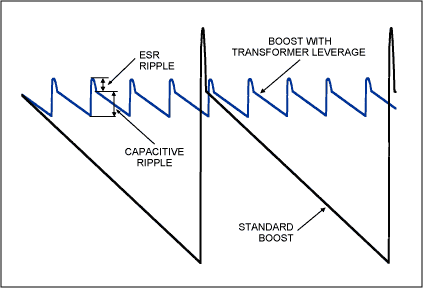
Figure 5. This illustration contrasts the ripple produced by the circuit of Figure 1a vs. the circuit of Figure 1c assuming both are optimized for a minimum acceptable off-time.
The percent efficiency loss due to DC resistance in the switch and in the primary side of the transformer is independent of load, and can be approximated as:

where ER_LOSS is the energy loss due to resistance per pulse, and Edelivered is the energy delivered per pulse. By taking the integral of the primary-side resistive power dissipation, the resistive efficiency loss for large duty cycles can be approximated as:

where D is the duty cycle expressed as a percentage, and R is the sum of the switch resistance and the primary-side resistance. For operation in discontinuous mode, the same equation applies for the circuit of Figure 1a or 1c. The efficiency loss due to leakage inductance can be approximated as:

where Lleakage is the total leakage inductance seen at the primary side. Transformers with higher turns ratios provide larger leakage inductance, higher frequency, and deliver lower energy per pulse, so the source of inefficiency becomes more significant.
When specifying an autotransformer, consider an equivalent inductor. The following inductor, for example, is available from Tok
D32FU 680 µH, 74mA, 20Ω, 3.5mm × 3.5mm × 2.2mm.
It is reasonable to ask for an autotransformer whose end-to-end characteristics are similar. For such a transformer with a 1:9 turns ratio, the primary-side rating would be 6.8 µH, 740mA, and 2Ω. That inductance rating is based on a value of N² (where N is the total number of turns divided by the number of primary-side turns). For a 1:9 turns ratio there must be some multiple of 10 turns total. N = 10 must be used for the previous calculation. The saturation current is inversely proportional to N and resistance is proportional to N.
Occasionally, thermal limitations do not allow the maximum current rating to scale by N. Also, a limited product selection may bar you from that ideal starting point. This analysis provides a starting point and a decent edge when discussing possibilities with a custom transformer vendor. When wound as an autotransformer, an equivalent magnetic component should require less space (a smaller wiring cavity) because the lower currents allow thinner wire on the secondary side. Extra manufacturing costs usually prohibit this approach, however.

Figure 6. This circuit, whose layout is shown in Figure 2, is used to produce 75V from 2.5V.
Figure 7 shows the MAX1605 maximum output current (the measured typical,for which the controller falls out of regulation by 5") as a function of output voltage and input voltage.
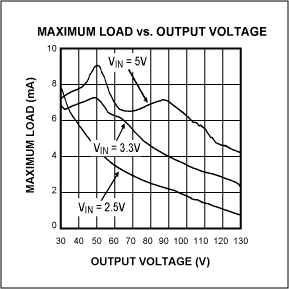
Figure 7. This maximum load vs. output voltage graph illustrates the maximum load deliverable by the circuit of Figure 6.
Output ripple for the circuit of Figure 1c can be calculated as:

where LP is the primary-side inductance, IPK is the peak primary-side current (500mA), COUT is the output capacitance (0.47µF), and VOUT is the output voltage. For a 75V output, the ripple is 16mVP-P. The low inductance that produces such a low ripple is typically not efficient in a straight boost configuration like Figure 1a.
Even 16mVP-P ripple is not small enough for many applications.To bias an APD, high ripple is unacceptable because it couples directly into the signal. Such applications can use an RC or LC filter following the power supply, but the resistor in an RC filter produces a load-regulation error. Typical load currents are small, but the ripple filter may require large resistors.
At 100V, high-capacitance values require board space, so the filter is composed largely of resistance. For the same cutoff frequency (using the same resistor and capacitor), you can reduce the load-regulation error by a factor of β using the circuit of Figure 8. Although a fixed VBE drop is introduced instead, that approach dramatically reduces the dependence of VOUT on load. To achieve greater ripple reduction for the same level of load regulation, a β-times larger filter resistor can be used.
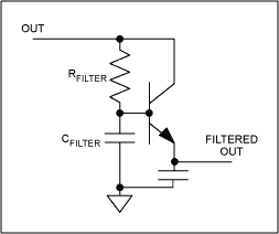
Figure 8. A filter further reduces ripple.
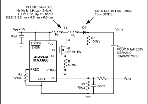
Figure 9. This circuit can be used to deliver higher power and higher output voltage.
The MAX668 includes a MOSFET driver that can efficiently drive the 48nC gate charge of an IRF7401 MOSFET. With the following components, it forms a 150V inductor-based boost converter.The following components were used in conjunction with the MAX668 Evaluation Kit:
For the inductor-based solution, the maximum load current is 18mA at 150V (2.7W). Peak efficiency (65") occurs at maximum load and the quiescent (no-load) current is 91mA with a 6V supply. The quiescent current loss in the inductor circuit is due to the diode's reverse-recovery time and the MOSFET's drain capacitance. Those effects are illustrated in Figure 10 .
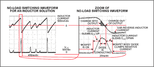
Figure 10. This scope photo (left) demonstrates the effect of the ES1D diode's 15ns reverse-recovery time. The zoom of the waveform (right) reveals that the inductor current actually ramps negative since the diode fails to turn off in time.
The transformer-based approach (Figure 11) was implemented by exchanging the inductor for the following transformer, using the topology of Figure 1c:
Sumida CMD-8LN 6313-T036,
LP = 5.6µH, IP = 2.3A, NP:NS = 1:9,
RP = 0.5Ω
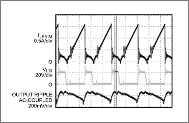
Figure 11. The switching waveform shows the transformer-based approach for the MAX668 circuit, a 150V step-up DC-DC converter shown in Figure 9.
Using a transformer with a 1:9 turns ratio requires only a 22V MOSFET, but an actual application would use a 30V MOSFET (instead of a 200V MOSFET) for the transformer circuit. Yet, the efficiency is 77" while delivering 25.5mA at 150V (3.8W). Peak efficiency is 88" at 15mA, and the no-load supply current is only 1.8mA total.
Using the 200V MOSFET with a transformer allows the possibility of much higher voltage. A 200V MOSFET and 1:9 transformer can approach output voltages as high as 2kV in theory, but in practice the transformer windings cannot sustain such high voltage. A greater problem, however, is obtaining >1kV diodes with fast reverse-recovery times. For slow reverse-recovery times, the switching speed must be reduced.
Substituting a 400V CMR1U-04 diode from Central Semiconductor (50ns tRR) for the ES1D diode and changing the output capacitors allows the circuit to produce outputs as high as 400V. The ES1D diode cannot reliably produce outputs greater than 346V, because its anode goes to -9 × VIN when the MOSFET turns on. Configured for VOUT= 330V, the circuit was able to produce 9.6mA (3.1W) at 60" efficiency and the peak efficiency was 66" at 4mA.
As mentioned earlier, a 30V MOSFET is more logical for the 150V output. The IRF640NS was replaced with a logic-level IRF7811W (30V, 0.012Ω, QG = 18nC, CDSS = 500pF). Resistance drops dramatically (from 0.15Ω to 0.012Ω), but the efficiency improvement is minor. When delivering a maximum load of 25.7mA at 150V, the efficiency is 82.3" (vs.77"). Peak efficiency at 15.5mA is 88". Efficiency results are summarized in Figure 12.
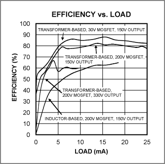
Figure 12. This efficiency vs. load graph compares and contrasts transformer-based, step-up DC-DC converters vs. inductor-based, step-up DC-DC converters. The maximum load, quiescent current, and efficiency are greatly improved using a transformer.
The insignificant improvement in efficiency implies two things. Primary losses are in the transformer (resistive loss and leakage energy), and capacitive losses are in the MOSFET. The dominant loss is associated with the transformer's primary-side resistance, which is about 0.5Ω. You can scale this system to provide higher power. For example, another custom transformer specified for IPSAT = 5A and LP = 1.7 µH should deliver more than twice as much power.
Thus, besides use of the smaller, cheaper, and more efficient IRF7811W MOSFET, a transformer boost converter can operate with lower input voltages. Transformer leverage can improve power density and efficiency, reduce ripple, and allow the use of smaller, cheaper, and sometimes internal MOSFETS. The cost of applying transformer leverage is mostly due to market limitations. When size and power density are a high priority, consider using transformers.

Figure 1a-1c. These high-voltage DC-DC converters in three topologies are used to create high output voltage from low input voltage.
The high-voltage bias required in many APD applications (75V) is derived from a 3V supply. That requirement presents the following challenges:
- High-voltage MOSFETs generally do not operate with a low 3V gate drive.
- The larger drain-source capacitance of high-voltage MOSFETs requires energy in the inductor to slew the drain to the output voltage. The resulting losses are as large as 1/2 fswitch×CDSVOUT ².
- High-voltage MOSFETs are larger and more expensive than their lower voltage counterparts. High-voltage power MOSFETs are seldom found within switching-controller ICs.
- Extreme duty cycles impose inefficiently small off-times or low switching frequencies. Lower switching frequency causes higher ripple and requires larger magnetics.
Figure 2. This 6mm x 8.5mm DC-DC converter converts 2.5V to 75V using the MAX1605. The front and back layout of the circuit is shown.
Theory of Operation
Standard boost and flyback DC-DC converters can be merged to form the hybrid topology of Figure 1c. The resulting merged topology stacks secondary-winding flyback voltage on top of the input voltage and the primary-winding flyback voltage (a standard flyback converter only takes advantage of flyback voltage produced at the secondary side). Compared with a standard boost converter,this topology produces higher output voltages from a lower voltage MOSFET by limiting the voltage seen at LX.A transformer provides the following advantages:
- Higher attainable output voltage
- Lower operating duty cycle
- Lower voltage on the MOSFET
- Higher switching frequency produces lower output ripple
- Higher frequency ripple
- Smaller magnetics
Standard Boost
The standard boost converter is shown in Figure 1a. When the MOSFET turns on, the inductor current ramps up. When the MOSFET turns off, LX flies up to VOUT + VD, and the inductor current ramps down. Intuitively, if the inductor spends 1/nth of its time delivering energy to the output, the output voltage (VOUT) is n times the input voltage (VIN), thus the following equation can be generated:
where D is the duty cycle. A more analytical proof can be found by using Figure 3. The key to this proof lies in steady-state operation, for which the current must ramp down the same amount that it ramps up:


Figure 3. This analysis of the inductor current for the circuit of Figure 1a can be used to determine its duty cycle.
Thus, the final inductor current equals the initial inductor current:

Because they are equal,

The circuit of Figure 1b could be made equivalent to the circuit of Figure 1a by connecting the left side of the transformer's secondary winding to VIN and setting the turns ratio to 1. The secondary-side diode can be reflected to the primary side, making the relationship between a flyback converter and a boost converter easier to perceive.
Turns ratios larger than 1:1 provide leverage by allowing higher output voltage with less extreme duty cycles. Alternatively, node 1 of the transformer can be connected to any power supply, enabling leverage with respect to that supply. Because LX flies up during the off-cycle, an additional voltage step can be obtained by connecting node 1 to LX, as shown in Figure 1c. That connection also helps catch some of the leakage energy that would otherwise be dumped from the transformer's primary side to the MOSFET, producing short, high-voltage spikes at the MOSFET's drain. If the voltage spikes are higher than the MOSFET's voltage tolerance, a snubber circuit will be necessary to dissipate the leakage energy.
LX is shorted to ground in Figure 1b, allowing the primary-side current to ramp up as for an inductor. No current flows through the secondary side of the transformer and the diode is reverse-biased because

Primary-side current must cease when the switch at LX turns off, but the N × I product must remain constant:

where subscript "P" indicates primary side, subscript "S" indicates secondary side, "initial" indicates current at the moment before the MOSFET is switched off, and "final" indicates current at the moment after the MOSFET is switched off.
Because IS_initial = IP_final = 0,

The circuit of Figure 1c is similar, except that IP_final = IS_final, so

To simplify, the turns ratio 'N' is expressed as:

because the secondary side of Figure 1c never acts independently. Though unconventional, this definition for N is more appropriate for Figure 1c.
Figure 4 shows the primary-side current waveform for Figure 1c. For step-up converters whose output is more than twice the input voltage, off-time has a greater effect on the efficiency than on-time. Assume (for a comparable boost converter) that off-time has been minimized by minimizing inductance (LBST), which also minimizes component size to the point that further reduction would lead to undesired efficiency loss. Then, select the Figure 4 transformer's total inductance to be N times as large. Because the primary-side current ramps down from IPK/N instead of IPK, the primary inductance must be N times as large to maintain the same off-time.

Figure 4. This analysis of the primary-side transformer current for the circuit of Figure 1c can be used to determine its duty cycle.
The primary-side inductance is:

where LTOT is the total inductance of the autotransformer since LBST is N² smaller than LTOT, and LTOT is N times larger than LBST, LP is LBST/N. As a result, the primary side ramps faster than a simple boost converter.

For the steady state, it is clear from Figure 4 that:

where ΔIUP is the upward step in the primary-side current and ΔIDOWN is the downward step. ΔIUP and ΔIDOWN can be calculated as follows:

and

so

Solving for VOUT/VIN yields:

Figures 3 and 4 are both drawn to scale and have the same off-time (set to some optimal minimum). The shaded regions in Figures 3 and 4 represent energy delivered to the load, and the energy per pulse is proportional to the area of those regions. That energy can also be calculated from the expression 1/2 L × I² (note that L in Figure 4 is N times larger, and I is N times smaller). Because the circuit of Figure 1c delivers less energy per pulse, the ripple is N times smaller. Thus, a transformer not only leverages the output voltage up; it also leverages the output ripple down.
The topology of Figure 1c delivers less energy per pulse, but compensates by delivering more pulses, as clearly indicated in Figure 4. Figure 1c requires an N times larger inductance, but the saturation current can be N times smaller because the primary and secondary side see only IPK/N as much current simultaneously. With an ISAT smaller by a factor of N and an inductance N times larger, the transformer's energy-storage capability may also be N times smaller. Transformer size is a function of its energy-storage capability, so in theory you can use a transformer that is physically smaller by a factor of N. In practice, the attainable size is determined by market limitations.
Output Ripple
For discontinuous conduction, either converter's output ripple can be calculated by equating energy change in the inductor or transformer with energy change in the output capacitor during the off-cycle. Because the inductor/transformer has zero energy at the end of the cycle, no-load ripple can be calculated as:
For the boost converter L = LBST and I = IPK. For the circuit of Figure 1c, L = LBST × N and I = IPK/N, s

where ΔVOUTA is the output ripple of the boost configuration, and ΔVOUTC is the output ripple for the Figure 1c circuit. Ripple in Figure 1c is 1/Nth as large for the boost configuration and the switching frequency is N times higher.
Figure 5 offers a comparison of ripple for the circuits of Figures 1a and 1c, when both circuits are designed for the same off-time. Because the duty cycle is normalized in the transformer circuit (made closer to 50"), the controller can operate at a frequency N times higher for the same off-time.

Figure 5. This illustration contrasts the ripple produced by the circuit of Figure 1a vs. the circuit of Figure 1c assuming both are optimized for a minimum acceptable off-time.
Efficiency Considerations
There are three main efficiency losses to consider in the transformer topology. Transformer/inductor DC resistance combined with switch resistance produces losses proportional to the square of the peak current. Transformer-leakage inductance produces loss because transformer energy is not completely coupled to the output. When the diode is quickly and heavily reverse-biased (when the MOSFET turns on), any delay in the diode (the reverse-recovery time, tRR) can also cause significant loss.The percent efficiency loss due to DC resistance in the switch and in the primary side of the transformer is independent of load, and can be approximated as:

where ER_LOSS is the energy loss due to resistance per pulse, and Edelivered is the energy delivered per pulse. By taking the integral of the primary-side resistive power dissipation, the resistive efficiency loss for large duty cycles can be approximated as:

where D is the duty cycle expressed as a percentage, and R is the sum of the switch resistance and the primary-side resistance. For operation in discontinuous mode, the same equation applies for the circuit of Figure 1a or 1c. The efficiency loss due to leakage inductance can be approximated as:

where Lleakage is the total leakage inductance seen at the primary side. Transformers with higher turns ratios provide larger leakage inductance, higher frequency, and deliver lower energy per pulse, so the source of inefficiency becomes more significant.
Transformer Selection
Since the selection of off-the-shelf transformers is much narrower than that of equivalent inductors, transformers generally cost more than inductors of equivalent energy and energy density. The customer base for transformers is smaller, yet the set of possible transformer configurations is much larger than that of corresponding inductor configurations. As a result, magnetic designs based on custom transformers are often necessary.When specifying an autotransformer, consider an equivalent inductor. The following inductor, for example, is available from Tok
D32FU 680 µH, 74mA, 20Ω, 3.5mm × 3.5mm × 2.2mm.
It is reasonable to ask for an autotransformer whose end-to-end characteristics are similar. For such a transformer with a 1:9 turns ratio, the primary-side rating would be 6.8 µH, 740mA, and 2Ω. That inductance rating is based on a value of N² (where N is the total number of turns divided by the number of primary-side turns). For a 1:9 turns ratio there must be some multiple of 10 turns total. N = 10 must be used for the previous calculation. The saturation current is inversely proportional to N and resistance is proportional to N.
Occasionally, thermal limitations do not allow the maximum current rating to scale by N. Also, a limited product selection may bar you from that ideal starting point. This analysis provides a starting point and a decent edge when discussing possibilities with a custom transformer vendor. When wound as an autotransformer, an equivalent magnetic component should require less space (a smaller wiring cavity) because the lower currents allow thinner wire on the secondary side. Extra manufacturing costs usually prohibit this approach, however.
Application
The circuit of Figure 6 produces an APD bias of 75V. Because the transformer reduces voltage stress on the switch, you can use a small 6-pin SOT23 device such as the MAX1605. The 28V, 500mA MOSFET in that IC is more than adequate since it only sees peak voltages of VIN + (VOUT - VIN)/N = 17V. With a higher turns ratio, the circuit can handle higher voltages.
Figure 6. This circuit, whose layout is shown in Figure 2, is used to produce 75V from 2.5V.
Figure 7 shows the MAX1605 maximum output current (the measured typical,for which the controller falls out of regulation by 5") as a function of output voltage and input voltage.

Figure 7. This maximum load vs. output voltage graph illustrates the maximum load deliverable by the circuit of Figure 6.
Output ripple for the circuit of Figure 1c can be calculated as:

where LP is the primary-side inductance, IPK is the peak primary-side current (500mA), COUT is the output capacitance (0.47µF), and VOUT is the output voltage. For a 75V output, the ripple is 16mVP-P. The low inductance that produces such a low ripple is typically not efficient in a straight boost configuration like Figure 1a.
Even 16mVP-P ripple is not small enough for many applications.To bias an APD, high ripple is unacceptable because it couples directly into the signal. Such applications can use an RC or LC filter following the power supply, but the resistor in an RC filter produces a load-regulation error. Typical load currents are small, but the ripple filter may require large resistors.
At 100V, high-capacitance values require board space, so the filter is composed largely of resistance. For the same cutoff frequency (using the same resistor and capacitor), you can reduce the load-regulation error by a factor of β using the circuit of Figure 8. Although a fixed VBE drop is introduced instead, that approach dramatically reduces the dependence of VOUT on load. To achieve greater ripple reduction for the same level of load regulation, a β-times larger filter resistor can be used.

Figure 8. A filter further reduces ripple.
Experimental Comparison, Inductor and Transformer Approaches
For a fair comparison of inductors versus transformers in a high-voltage converter, a switching converter with the following features was selected:- External MOSFETs
- Adjustable switching frequency
- Adjustable current limit
- Evaluation kit available

Figure 9. This circuit can be used to deliver higher power and higher output voltage.
The MAX668 includes a MOSFET driver that can efficiently drive the 48nC gate charge of an IRF7401 MOSFET. With the following components, it forms a 150V inductor-based boost converter.The following components were used in conjunction with the MAX668 Evaluation Kit:
- Inductor: Coilcraft DO1813P-472HC 4.7µH, 2.6A 0.054Ω inductor
- Ultra-fast diode: ES1D 200V 15ns reverse-recovery time
- MOSFET: IRF640NS 200V 0.15Ω QG = 67nC, COSS = 185pF, and provides over 2A with 5.5V gate drive
- Sense resistor: 50mΩ sense resistor
For the inductor-based solution, the maximum load current is 18mA at 150V (2.7W). Peak efficiency (65") occurs at maximum load and the quiescent (no-load) current is 91mA with a 6V supply. The quiescent current loss in the inductor circuit is due to the diode's reverse-recovery time and the MOSFET's drain capacitance. Those effects are illustrated in Figure 10 .

Figure 10. This scope photo (left) demonstrates the effect of the ES1D diode's 15ns reverse-recovery time. The zoom of the waveform (right) reveals that the inductor current actually ramps negative since the diode fails to turn off in time.
The transformer-based approach (Figure 11) was implemented by exchanging the inductor for the following transformer, using the topology of Figure 1c:
Sumida CMD-8LN 6313-T036,
LP = 5.6µH, IP = 2.3A, NP:NS = 1:9,
RP = 0.5Ω

Figure 11. The switching waveform shows the transformer-based approach for the MAX668 circuit, a 150V step-up DC-DC converter shown in Figure 9.
Using a transformer with a 1:9 turns ratio requires only a 22V MOSFET, but an actual application would use a 30V MOSFET (instead of a 200V MOSFET) for the transformer circuit. Yet, the efficiency is 77" while delivering 25.5mA at 150V (3.8W). Peak efficiency is 88" at 15mA, and the no-load supply current is only 1.8mA total.
Using the 200V MOSFET with a transformer allows the possibility of much higher voltage. A 200V MOSFET and 1:9 transformer can approach output voltages as high as 2kV in theory, but in practice the transformer windings cannot sustain such high voltage. A greater problem, however, is obtaining >1kV diodes with fast reverse-recovery times. For slow reverse-recovery times, the switching speed must be reduced.
Substituting a 400V CMR1U-04 diode from Central Semiconductor (50ns tRR) for the ES1D diode and changing the output capacitors allows the circuit to produce outputs as high as 400V. The ES1D diode cannot reliably produce outputs greater than 346V, because its anode goes to -9 × VIN when the MOSFET turns on. Configured for VOUT= 330V, the circuit was able to produce 9.6mA (3.1W) at 60" efficiency and the peak efficiency was 66" at 4mA.
As mentioned earlier, a 30V MOSFET is more logical for the 150V output. The IRF640NS was replaced with a logic-level IRF7811W (30V, 0.012Ω, QG = 18nC, CDSS = 500pF). Resistance drops dramatically (from 0.15Ω to 0.012Ω), but the efficiency improvement is minor. When delivering a maximum load of 25.7mA at 150V, the efficiency is 82.3" (vs.77"). Peak efficiency at 15.5mA is 88". Efficiency results are summarized in Figure 12.

Figure 12. This efficiency vs. load graph compares and contrasts transformer-based, step-up DC-DC converters vs. inductor-based, step-up DC-DC converters. The maximum load, quiescent current, and efficiency are greatly improved using a transformer.
The insignificant improvement in efficiency implies two things. Primary losses are in the transformer (resistive loss and leakage energy), and capacitive losses are in the MOSFET. The dominant loss is associated with the transformer's primary-side resistance, which is about 0.5Ω. You can scale this system to provide higher power. For example, another custom transformer specified for IPSAT = 5A and LP = 1.7 µH should deliver more than twice as much power.
Thus, besides use of the smaller, cheaper, and more efficient IRF7811W MOSFET, a transformer boost converter can operate with lower input voltages. Transformer leverage can improve power density and efficiency, reduce ripple, and allow the use of smaller, cheaper, and sometimes internal MOSFETS. The cost of applying transformer leverage is mostly due to market limitations. When size and power density are a high priority, consider using transformers.
 电子发烧友App










评论