Abstract: Analog-to-digital converter (ADC) data sheets and application typically recommend driving their inputs with a low source impedance. This application note explains the possible effects such as increased gain error and distortion when using high impedance to drive an ADC without a buffer.
Analog-to-digital converter (ADC) users have been instructed by endless data sheets and application notes to drive their ADCs with a low source impedance. However, these instructions often do not tell us what can happen if a low impedance is not used and what effects it can have on circuit performance. This article explains the principles behind and techniques for understanding the source of the distortion caused from a high source resistance on the input to an analog-to-digital converter.
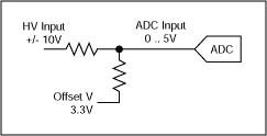
We can begin to understand the problem of high-source impedance effects by looking at the simple circuit below in Figure 1. It addresses a common need to scale a ±10V signal to a 0 to 5V ADC input with a simple voltage divider.

Figure 1. Scaling ADC input with a simple voltage divider.
For this circuit, the effective driving impedance into the ADC is the Thevenin equivalent impedance seen looking back into the divider, which equals the parallel combination of the divider resistors. This finite input resistance acts as a voltage divider with the input impedance of the ADC causing a low-frequency gain error as shown in Figure 2.
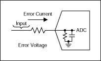
Figure 2. Error current and voltage due to finite input impedance.
In addition to the gain error, there are two other problems caused by this finite input resistance. The first is a settling time error. This is caused by the fact that the sampling capacitor is only allowed to charge for part of the sampling cycle, referred to the acquisition period. During this acquisition period the settling time will be increased due the additional time constant created by the input resistance and the input sampling capacitance. This error can be estimated by looking at the settling of a RC time constant using the input capacitance and the source impedance over the acquisition time period using the following equation:
The second error, which can sometimes be more critical than the gain errors discussed above, is distortion. The cause of this distortion can be understood by realizing that the input resistance and input capacitance of the ADC create a low-pass filter with a frequency dependant gain error. The distortion occurs due to the normal voltage dependant characteristic of the capacitor, meaning that the capacitance changes with the voltage applied. This characgteristic can be more pronounced in semiconductor process technology.
An equation that describes this change in one region of the voltage curve is:
C0 is the nominal capacitance,
V is the voltage across the capacitance,
K is a semiconductor process and design dependant constant.
A plot of a typical curve of this capacitance¹ is shown in Figure 3.
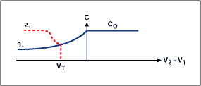
Figure 3. Variation of a capacitor with applied voltage.
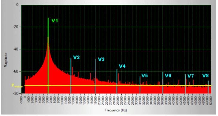
Referring back to Figure 2, this voltage-dependant capacitance causes the current necessary to charge the capacitance to vary with voltage (in addition to frequency). This current travels through the ADC driving impedance, which creates a voltage drop error, which again varies with voltage. If this error were independent of voltage, it would create a linear error, as discussed above. However, since it is voltage dependant, it creates a non-linear error. For a sine wave, this error contains harmonics. And, since this error originates as a current charging a capacitance, the error is non-existant at DC, and gets proportionately larger with frequency.
An example of the order of magnitude of this error for one ADC is that at 500kHz input frequency, 1kΩ source impedance, and full-scale input voltage yields a 70dB THD. This distortion component will approximately vary linearly with both impedance and frequency. For example, input frequencies and source impedance combinations of both (5MHz, 1kΩ) and (500kHz, 10kΩ) will be 10x or 20dB worse, yielding 50dB THD. Note, since this effect is highly dependant on both the design and semiconductor process, different ADCs can have radically different numbers. Hence, these numbers should not be applied towards any design.
There is no easy way to determine how much of a problem this is for your circuit because semiconductor manufacturers don't specify parameters like voltage-dependant input capacitance. The best advice is to follow the manufacturers recommendation for the maximum size of the input resistance required to meet the stated performance. It is always a good practice to always drive the input of the ADC with as low of an impedance as possible.
A better solution is to use the IC products that incorporate the above resistive divider on the IC. For these products, the effects of the source impedance has been accounted for, and/or compensated for by the IC design engineers to make sure the part meets its distortion specifications.
Examples of parts that have been pre-engineered for you to translate the higher input voltage onto an internal lower voltage include the MAX1159, MAX1189, MAX1132-35, and MAX1142-45. These converters have a variety of power voltages, and input voltages, and resolution (# of bits), as shown in the Table 1 below.
Table 1. List of ADCs from Maxim with Input Range Beyond the Voltage Rails
Analog-to-digital converter (ADC) users have been instructed by endless data sheets and application notes to drive their ADCs with a low source impedance. However, these instructions often do not tell us what can happen if a low impedance is not used and what effects it can have on circuit performance. This article explains the principles behind and techniques for understanding the source of the distortion caused from a high source resistance on the input to an analog-to-digital converter.
We can begin to understand the problem of high-source impedance effects by looking at the simple circuit below in Figure 1. It addresses a common need to scale a ±10V signal to a 0 to 5V ADC input with a simple voltage divider.

Figure 1. Scaling ADC input with a simple voltage divider.
For this circuit, the effective driving impedance into the ADC is the Thevenin equivalent impedance seen looking back into the divider, which equals the parallel combination of the divider resistors. This finite input resistance acts as a voltage divider with the input impedance of the ADC causing a low-frequency gain error as shown in Figure 2.

Figure 2. Error current and voltage due to finite input impedance.
In addition to the gain error, there are two other problems caused by this finite input resistance. The first is a settling time error. This is caused by the fact that the sampling capacitor is only allowed to charge for part of the sampling cycle, referred to the acquisition period. During this acquisition period the settling time will be increased due the additional time constant created by the input resistance and the input sampling capacitance. This error can be estimated by looking at the settling of a RC time constant using the input capacitance and the source impedance over the acquisition time period using the following equation:
Ratio of Settling = 1-e-(Tacquisition/RC)This is mostly a linear error, but can have some non-linear components.
The second error, which can sometimes be more critical than the gain errors discussed above, is distortion. The cause of this distortion can be understood by realizing that the input resistance and input capacitance of the ADC create a low-pass filter with a frequency dependant gain error. The distortion occurs due to the normal voltage dependant characteristic of the capacitor, meaning that the capacitance changes with the voltage applied. This characgteristic can be more pronounced in semiconductor process technology.
An equation that describes this change in one region of the voltage curve is:
C = C0 × ( 1 + K × V- ),where
C0 is the nominal capacitance,
V is the voltage across the capacitance,
K is a semiconductor process and design dependant constant.
A plot of a typical curve of this capacitance¹ is shown in Figure 3.

Figure 3. Variation of a capacitor with applied voltage.
Referring back to Figure 2, this voltage-dependant capacitance causes the current necessary to charge the capacitance to vary with voltage (in addition to frequency). This current travels through the ADC driving impedance, which creates a voltage drop error, which again varies with voltage. If this error were independent of voltage, it would create a linear error, as discussed above. However, since it is voltage dependant, it creates a non-linear error. For a sine wave, this error contains harmonics. And, since this error originates as a current charging a capacitance, the error is non-existant at DC, and gets proportionately larger with frequency.
An example of the order of magnitude of this error for one ADC is that at 500kHz input frequency, 1kΩ source impedance, and full-scale input voltage yields a 70dB THD. This distortion component will approximately vary linearly with both impedance and frequency. For example, input frequencies and source impedance combinations of both (5MHz, 1kΩ) and (500kHz, 10kΩ) will be 10x or 20dB worse, yielding 50dB THD. Note, since this effect is highly dependant on both the design and semiconductor process, different ADCs can have radically different numbers. Hence, these numbers should not be applied towards any design.
There is no easy way to determine how much of a problem this is for your circuit because semiconductor manufacturers don't specify parameters like voltage-dependant input capacitance. The best advice is to follow the manufacturers recommendation for the maximum size of the input resistance required to meet the stated performance. It is always a good practice to always drive the input of the ADC with as low of an impedance as possible.
A better solution is to use the IC products that incorporate the above resistive divider on the IC. For these products, the effects of the source impedance has been accounted for, and/or compensated for by the IC design engineers to make sure the part meets its distortion specifications.
Examples of parts that have been pre-engineered for you to translate the higher input voltage onto an internal lower voltage include the MAX1159, MAX1189, MAX1132-35, and MAX1142-45. These converters have a variety of power voltages, and input voltages, and resolution (# of bits), as shown in the Table 1 below.
Table 1. List of ADCs from Maxim with Input Range Beyond the Voltage Rails
|
|
|
Selectable Input Range |
|
|
(KSPS) |
|
|
|
|
|
|
|
|
|
|
|
|
|
|
|
|
|
|
|
|
|
|
|
|
|
|
|
|
|
|
|
|
|
|
|
|
|
|
|
|
|
|
|
|
|
|
|
|
|
|
|
|
|
|
|
|
|
|
|
|
|
|
|
|
|
|
|
|
|
|
|
|
|
|
|
|
|
|
|
|
|
|
|
|
|
|
|
|
|
|
|
|
|
|
|
|
|
|
|
|
|
|
|
|
|
|
|
|
|
|
|
|
|
|
|
|
|
|
|
|
|
|
|
|
|
|
|
|
|
|
|
|
|
|
|
|
|
|
|
|
|
|
|
|
|
|
|
|
|
|
|
|
|
|
|
|
|
|
|
|
|
 电子发烧友App








评论