Abstract: Sensor compensation has historically been based on an analog architecture. The advent of high-performance calculating engines for digital-sensor signal processing (DSSP) has recently made such architectures available for use in pressure sensors. As a result, the next generation of integrated circuits (ICs) for conditioning and converting pressure-transducer outputs will incorporate the DSSP architecture. This application note details the DSSP architecture as used in the MAX1460 sensor signal conditioner.
The leading consumer of the silicon-based pressure sensors called MEMS (micro-electro mechanical sensors) continues to be the automotive market. In 1999, sensors comprised 12% of the $10.67 billion spent for automotive electronics (source: Strategic Analytics). This trend should continue as sensor development expands the existing applications and enables new automotive features. Of the new signal-processing and signal-conversion architectures being introduced in the automotive market, one in particular (the MAX1460) enables a greater level of sensor performance with existing MEMS-based transducers.
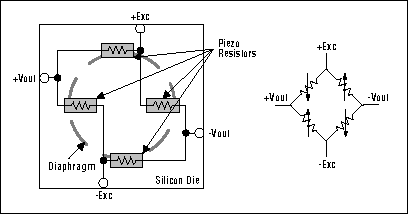
Figure 1. A typical silicon pressure transducer has the equivalent circuit shown at right.
In a bridge configuration, the resistance of diagonally opposed legs varies equally and in the same direction, as a function of the mechanical deformation caused by pressure. As the resistance of one set of diagonally opposed legs increases under pressure, the resistance of the other set decreases, and vice versa. Bridge excitation in the form of voltage or current is applied across two opposite corners of the bridge. Shown as +Exc and -Exc in Figure 1, these terminals are usually called "excitation inputs" or "bridge-drive inputs."
Any change in resistance (that is, pressure) is detected as a voltage difference across the other two corners of the bridge (+Vout and -Vout in Figure 1), which are typically called the "bridge output"or the "signal output." Unfortunately for silicon piezoresistive sensors, this voltage difference is quite small (tens of millivolts). What's more, the full-span output (FSO) of an uncompensated sensor can exhibit a strong nonlinear dependence on temperature, a large initial offset (up to 100% of FSO or more), and a strong drift of offset with temperature. FSO is defined as the difference in sensor outputs corresponding to the maximum and minimum applied pressures. Thus, a sensor must be compensated before it can be used.
Sensors incorporating an integrated circuit for compensation have been around for many years. Generally, this compensation has been based on an analog architecture (referred to here as analog-sensor signal processing, or ASSP). The advent of fine-geometry CMOS and high-performance calculating engines for digital-sensor signal processing (DSSP) has recently made such architectures available for use in pressure sensors. As a result, the next generation of ICs for conditioning and converting pressure-transducer outputs will incorporate the DSSP architecture.
These architectures were used in engine-management modules to process data representing barometric air pressure (BAP) and manifold air pressure (MAP). These designs performed calibration and compensation in the analog domain. To store the sensor-specific data, analog "memory" components such as potentiometers, discrete resistors or capacitors (some of them temperature-dependent), and laser-trimmed resistors were used. Among the major problems with this approach are the following:
Two factors limited the performance of early designs: the use of low-resolution (8- and 10-bit) DACs and the use of a discrete temperature-sensing device connected to the signal-conversion IC. The second-wave architecture was enhanced tremendously by the introduction of 12- and 16-bit DACs and by the integration of a ratiometric temperature sensor into the IC. First-order temperature compensation, in which the temperature signal is local to the IC itself, is performed entirely by the signal-conversion IC. Sensor performance was increased by 2% or more over the typical automotive operating temperature range (-40°C to 125°C) and by as much as 0.1% in industrial applications.
As background, consider that several key factors are essential in making this third-wave architecture successful:
Evaluation of this equation requires addition and multiplication. Though not explicitly obvious from the equation, a third arithmetic operation (negation) is also required. To maintain the highest level of precision, all arithmetic operations should be performed at the resolution of the input signal, which in this case is 16 bits.
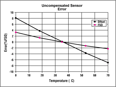
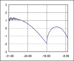
Figure 2. A slight curvature indicates second-order effects in the output of this piezoresistive transducer.
A new device, the MAX1460, is now available to perform the arithmetic operations required to compensate pressure sensors through the use of equation 1. Because this device can perform these arithmetic operations (using its on-board processor) on the pressure-sensor signal digitized with its on-board ADC, it is called a Smart-ADC?. See Figure 3.
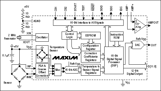
Figure 3. This drawing combines a block diagram and an application schematic for the MAX1460 signal conditioner.
A similar version of this article appeared in the January, 2001 issue of Sensor magazine.
The leading consumer of the silicon-based pressure sensors called MEMS (micro-electro mechanical sensors) continues to be the automotive market. In 1999, sensors comprised 12% of the $10.67 billion spent for automotive electronics (source: Strategic Analytics). This trend should continue as sensor development expands the existing applications and enables new automotive features. Of the new signal-processing and signal-conversion architectures being introduced in the automotive market, one in particular (the MAX1460) enables a greater level of sensor performance with existing MEMS-based transducers.
Characteristics of MEMS Pressure Transducers
Most of today's MEMS pressure transducers produced for the automotive market consist of a four-resistor Wheatstone bridge fabricated on a single monolithic die using bulk-etch micromachining technology. The piezoresistive elements integrated into the sensor die are located along the periphery of the pressure-sensing diaphragm at the points appropriate for strain measurement (see Figure 1). These sensors are inexpensive, because they are processed as integrated circuits, on a wafer that may contain a few hundred to a few thousand sensing elements.
Figure 1. A typical silicon pressure transducer has the equivalent circuit shown at right.
In a bridge configuration, the resistance of diagonally opposed legs varies equally and in the same direction, as a function of the mechanical deformation caused by pressure. As the resistance of one set of diagonally opposed legs increases under pressure, the resistance of the other set decreases, and vice versa. Bridge excitation in the form of voltage or current is applied across two opposite corners of the bridge. Shown as +Exc and -Exc in Figure 1, these terminals are usually called "excitation inputs" or "bridge-drive inputs."
Any change in resistance (that is, pressure) is detected as a voltage difference across the other two corners of the bridge (+Vout and -Vout in Figure 1), which are typically called the "bridge output"or the "signal output." Unfortunately for silicon piezoresistive sensors, this voltage difference is quite small (tens of millivolts). What's more, the full-span output (FSO) of an uncompensated sensor can exhibit a strong nonlinear dependence on temperature, a large initial offset (up to 100% of FSO or more), and a strong drift of offset with temperature. FSO is defined as the difference in sensor outputs corresponding to the maximum and minimum applied pressures. Thus, a sensor must be compensated before it can be used.
Sensors incorporating an integrated circuit for compensation have been around for many years. Generally, this compensation has been based on an analog architecture (referred to here as analog-sensor signal processing, or ASSP). The advent of fine-geometry CMOS and high-performance calculating engines for digital-sensor signal processing (DSSP) has recently made such architectures available for use in pressure sensors. As a result, the next generation of ICs for conditioning and converting pressure-transducer outputs will incorporate the DSSP architecture.
Analog-Sensor Signal Processing (ASSP)
The first generation of ICs to integrate ASSP usually included little more than differential to single-ended amplifiers. All of the transducer's performance peculiarities were amplified and passed on, leaving the transducer manufacturer to carry the burden of establishing sensor performance. Typically, the pressure-sensor signal and the temperature signal were presented to an electronic control unit (ECU), which used look-up tables to obtain a reasonable estimate of the pressure.These architectures were used in engine-management modules to process data representing barometric air pressure (BAP) and manifold air pressure (MAP). These designs performed calibration and compensation in the analog domain. To store the sensor-specific data, analog "memory" components such as potentiometers, discrete resistors or capacitors (some of them temperature-dependent), and laser-trimmed resistors were used. Among the major problems with this approach are the following:
- Restricted accuracy of compensation resulting from the sensor's nonlinearity
- High cost of laser trimmers and other automated equipment
- Multiple setups usually required for test and trim
- High component count preventing miniaturization
Two factors limited the performance of early designs: the use of low-resolution (8- and 10-bit) DACs and the use of a discrete temperature-sensing device connected to the signal-conversion IC. The second-wave architecture was enhanced tremendously by the introduction of 12- and 16-bit DACs and by the integration of a ratiometric temperature sensor into the IC. First-order temperature compensation, in which the temperature signal is local to the IC itself, is performed entirely by the signal-conversion IC. Sensor performance was increased by 2% or more over the typical automotive operating temperature range (-40°C to 125°C) and by as much as 0.1% in industrial applications.
Digital-Sensor Signal Processing (DSSP)
The third-generation DSSP architectural style is characterized by a fully digital compensation and error-correction scheme. Very-fine-geometry, mixed-signal CMOS IC technologies have enabled the incorporation of a sophisticated digital signal processor (DSP) into the sensor-compensator IC. The DSP was designed specifically for carrying out sensor-compensation calculations, enabling the sensor output to realize all the precision inherent in the transducer. Theoretically, linearizing the first- and second-order temperature effects on full-span output (FSO) and offset can make the overall linearity versus temperature better than that of the transducer itself.As background, consider that several key factors are essential in making this third-wave architecture successful:
- Transducer repeatability over temperature and pressure
- High-resolution A/D conversions (16-bit minimum)
- Computational engine with 16-bit multiplication and addition
- Synchronous operation between digital logic and signal-conversion circuits
- Ratiometric operation for all analog signal-processing subsystems
- High-resolution (12-bit minimum) D/A converters
- Low power consumption
- Transducer stability, repeatability, and hysteresis cannot be improved by calculation.
- Calculations can degrade but never increase the signal resolution.
- Output signal precision will be less than input signal resolution.
DOUT = Gain × (1/2 + G1× T + G2 × T²) × (Signal + Of0 + Of1× T + Of2 × T²) + DOFF (1), where
| DOUT | Compensated output signal |
| Gain | Compensates the output span |
| G1 | Compensates the first-order gain-temperature-coefficient (TC) errors |
| T | Temperature (expressed in °C) |
| G2 | Compensates the second-order gain-TC errors |
| Signal | Digitized representation of uncompensated transducer signal |
| Of0 | Compensates the transducer element's offset |
| Of1 | Compensates the first-order offset-TC errors |
| Of2 | Compensates the second-order offset-TC errors |
| DOFF | Zero-pressure output level |
Evaluation of this equation requires addition and multiplication. Though not explicitly obvious from the equation, a third arithmetic operation (negation) is also required. To maintain the highest level of precision, all arithmetic operations should be performed at the resolution of the input signal, which in this case is 16 bits.

Figure 2. A slight curvature indicates second-order effects in the output of this piezoresistive transducer.
A new device, the MAX1460, is now available to perform the arithmetic operations required to compensate pressure sensors through the use of equation 1. Because this device can perform these arithmetic operations (using its on-board processor) on the pressure-sensor signal digitized with its on-board ADC, it is called a Smart-ADC?. See Figure 3.

Figure 3. This drawing combines a block diagram and an application schematic for the MAX1460 signal conditioner.
A similar version of this article appeared in the January, 2001 issue of Sensor magazine.
 电子发烧友App










评论