Pushing the Limits of Packaging
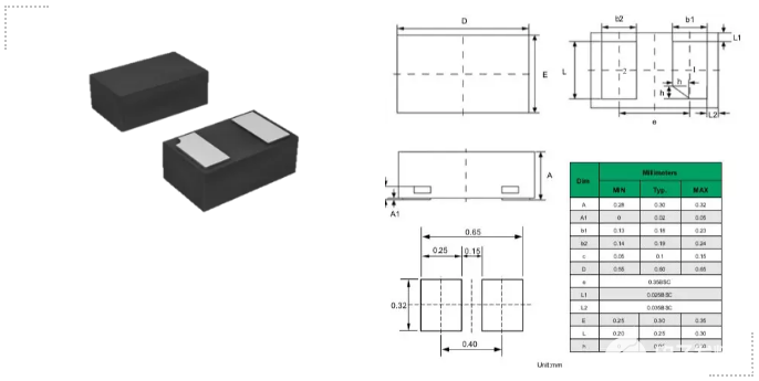
Packaging of microcontrollers plays a key role in the miniaturization of a system. The tradeoff of the choice of peripherals on the die, the pad count and the die size all limit the ability to reduce the size of the microcontroller, but nevertheless help reduce the overall size of the end equipment. Thermal issues are also important to consider as microcontrollers get smaller in size. With more transistors on a small die, running at higher frequencies, the power dissipation is a key consideration. While reducing the voltage and gating the different peripherals so that unused elements are not consuming power can reduce the overall thermal load, the excess heat generated must then be efficiently removed or the microcontroller will degrade and ultimately fail. This is a key reliability issue that has to be considered in miniaturizing the microcontroller system. This is where the tradeoff of pins versus size comes in. Additional pins on a package can be used to connect to thermal vias to take excess heat away from the microcontroller and other devices that may be sensitive to elevated temperatures such as a wireless interface. While the latest chip-scale packaging can reduce the overall footprint of a device with a given functionality, reducing the area taken up by a quarter, the opportunity to integrate more peripherals into a device and have more pins for thermal dissipation may be more important. The designer also has to be aware of the aim of miniaturization. An ARM 32-bit core, such as the Cortex-M0+ or even the M4, is less than a square millimeter of silicon – the size of the die is determined more by the amount of memory on chip and, vital for the packaging consideration, the peripherals that need to connect to the outside world. The smallest M0 devices, such as Freescale’s Kinetis KL02, can be as small as 1.9 x 2.0 mm in a chip-scale package that is barely larger than the die itself. At less than 4 square millimeters, this occupies twenty-five percent less PCB area than ball grid array or LGA packages but provides sixty percent more GPIO with up to twenty-eight lines. This move, almost 'silicon dust', allows designers to dramatically reduce their board size without compromising the performance, feature integration and power consumption of the end products.
Figure 1: The Kinetis KL02 family in chip-scale packaging provides a full microcontroller in a few square millimeters. Power consumption and thermal considerations are key at this size, and there are many things that can be done on the chip to reduce overall power dissipation and allow for a smaller package. The core runs at 48 MHz, helping to keep the power down over the whole -40°C to +105°C temperature range and allows the devices to be used in as many different environments as possible. There are also multiple low-power modes such as a new compute mode that reduces dynamic power by placing peripherals in an asynchronous stop mode. The Low-Power UART (LPUART), SPI, I²C, data converters, low-power timer and DMA engine all support a low-power mode operation where they operate without waking up the core. However, this does not necessarily reflect the actual use of silicon. Making many different versions of a microcontroller with a wide range of peripherals and memory options is actually expensive if separate masks are required. Instead, a single design with a superset of functions is implemented and manufactured, and only a specific set of features connected. This allows the silicon vendor to provide a wide range of products while minimizing the manufacturing costs and benefiting from economies of scale. The next stage of development has been to create a more flexible I/O configuration. Just as an internal bus matrix connects the peripherals, (as in the Atmel 4S family) so vendors are also introducing designs with a matrix that connects the I/O pins. This allows any peripheral to connect to any I/O pin, providing more flexibility for the vendor to deliver a family of pin-compatible devices where the same I/Os are always in the same place. As there is silicon to spare, this helps the system designer have a design with scalable performance without impacting on the overall size. All this means that the packaging technology is the key to the miniaturization of the microcontroller. Atmel has developed the SAM G51 series of Flash microcontrollers that is also based on the M4 core with floating point support. This also operates at a maximum speed of 48 MHz and features up to 256 Kbytes of Flash and up to 64 Kbytes of SRAM. The peripheral set includes one USART, two UARTs, two TWIs, one high-speed TWI, up to two SPIs, one three-channel general-purpose 16-bit timer, one RTT and one 8-channel, 12-bit ADC, greatly driving up the pin count requirements.
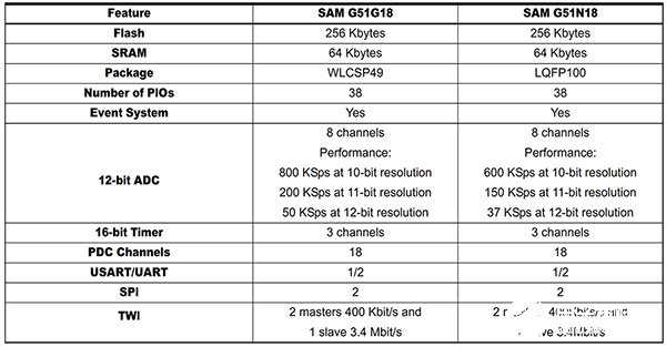
Figure 2: The Atmel SAM G51 family of microcontrollers showing the range of package options. This peripheral set allows the SAM G51 series to target a wide range of applications including consumer, industrial control, and PC peripherals with just two package types – a 49-ball WLCSP chip-scale package or a 100-lead LQFP package. At the same time, Atmel's SAM4S series is also based on the ARM Cortex-M4 processor core. It operates at higher maximum speed of 120 MHz and features up to 2048 Kbytes of Flash, with optional dual-bank implementation and cache memory, and up to 160 Kbytes of SRAM. The peripheral set includes a full-speed USB device port with embedded transceiver, a high-speed MCI for SDIO/SD/MMC, an external Bus interface with memory controller, two USARTs, two UARTs, two TWIs, three SPIs, one I²S, as well as one PWM timer, two three-channel general-purpose 16-bit timers (with stepper motor and quadrature decoder logic support), one RTC, one 12-bit ADC, one 12-bit DAC and one analog comparator. All of this brings even greater demands on the packaging and the pin count. The family has up to seventy-nine I/O lines with external interrupt capability (edge or level sensitivity), debouncing, glitch filtering and on-die series resistor termination, as well as three 32-bit Parallel Input/Output Controllers. This leads to a range of packages, from 100 leads down to 48 leads, but using the more traditional technologies: 100-lead packages
LQFP, 14 x 14 mm, pitch 0.5 mm TFBGA, 9 x 9 mm, pitch 0.8 mm VFBGA, 7 x 7 mm, pitch 0.65 mm
64-lead packages
LQFP, 10 x 10 mm, pitch 0.5 mm QFN, 9 x 9 mm, pitch 0.5 mm WLCSP, 4.42 x 3.42 mm, pitch 0.4 mm (SAM4S16/S8) WLCSP, 3.32 x 3.32 mm, pitch 0.4 mm (SAM4S4/S2)
48-lead packages
LQFP, 7 x 7 mm, pitch 0.5 mm QFN, 7 x 7 mm, pitch 0.5 mm
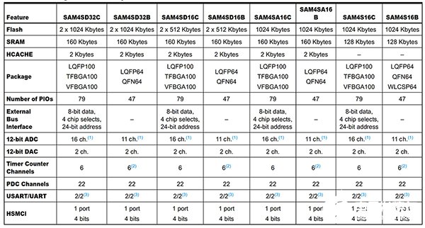
Figure 3: The Atmel SAM4S family has a much wider range of peripheral options leading to larger packages. Future trends New packaging technologies that stack die on top of each other in the same package also help to reduce the overall footprint. Instead of having a separate memory chip alongside the microcontroller, the microcontroller die is mounted on top of a memory die or large FPGA in one package. This approach, commonly called 2.5D, requires a silicon interposer and through silicon vias (TSVs) which is a relatively new technology that is now maturing and becoming more common. This is used in high-end devices that need larger amounts of memory that cannot be cost effectively integrated on a single die. Full 3D packaging sees multiple die stacked directly on top of each other; perhaps with I/O pads on the edges to allow interconnect between the different devices. While this has been a long-term aim of miniaturization, combining all the elements on a printed circuit board from the microcontroller to memory and wireless interface into one packaged device, it has yet to overcome a number of cost, reliability and thermal issues. Conclusion The wide range of microcontrollers from multiple vendors hides a strategy in the miniaturization of such devices. The range of packaging in different families from one vendor, all around the same core, demonstrates the complex tradeoff between footprint, peripheral mix, power, and system size. Further down the performance curve, 32-bit controllers with complex peripherals are now little more than a couple of square millimeters, becoming 'silicon dust' that permeates the Internet of Things.
破除封装的限制
包装微控制器起着一个系统的小型化的关键作用。在管芯的外围设备的选择的折衷,衬垫计数和芯片尺寸的所有限制,以减少微控制器的尺寸,但仍然有利于降低端设备的整体尺寸的能力。散热问题也是需要考虑的微控制器获得规模较小重要。与上一个小芯片更多的晶体管,运行在较高的频率时,功耗是一个关键的考虑因素。同时降低了电压门控和在不同的外设,使未使用的元件不消耗功率可以降低整体的热负荷,产生的多余热量必须再有效地去除或微控制器将降低并最终失败。这是一个关键的可靠性问题,有在小型化的微控制器系统中加以考虑。这就是销与大小的折衷用武之地。上一包的附加引脚可以用于连接到散热通孔采取多余的热量远离微控制器和其他设备可以是在升高的温度敏感诸如无线接口。而最新的芯片级封装可以减少设备的整体尺寸与给定的功能,从而减少了四分之一占据的区域,有机会更多外设集成到一个设备,并有更多的引脚用于热耗散可能更重要。设计者还必须知道的小型化的目的。
一个ARM 32位核,如在Cortex-M0 +或甚至在M4,小于硅的平方毫米 - 管芯的尺寸更受的存储器芯片的数量,并且对于包装考虑的重要决定,需要连接到外部世界的外设。最小M0设备,如飞思卡尔的Kinetis KL02,可以小如1.9×2.0毫米的芯片级封装,仅比管芯本身大。在小于4平方毫米,这占用较少的百分之二十五的PCB面积比球栅阵列或LGA封装,但提供的百分之六十以上的GPIO多达28行。此举,几乎是'硅尘“,使设计人员能够大幅降低其电路板尺寸不影响性能,功能集成的终端产品和功耗。
飞思卡尔的Kinetis KL02系列图1形象:Kinetis KL02系列的芯片级封装提供了一个完整的微控制器在几平方毫米。功率消耗和散热的考虑是,在这个尺寸键,并且存在可以在芯片上完成,以降低整体功耗,并允许更小的封装许多东西。核心运行在48兆赫,有助于保持掉电在整个-40°C到+ 105℃的温度范围内,并且允许设备在许多不同的环境中尽可能地使用。也有多个低功率模式,如新的计算模式,它使外围设备异步停止模式降低动态功耗。低功耗UART(LPUART),SPI,I²C,数据转换器,低功耗定时器和DMA引擎都支持,他们没有醒来的核心操作低功率模式操作。然而,这并不一定反映实际使用的硅。如果单独口罩都需要做许多不同版本的微控制器具有广泛的外设和存储器的选择实际上是昂贵的。相反,随着功能的一个超集的单个设计实现和制造,并且只有一组特定的连接的功能。这使得芯片供应商提供范围广泛的产品,同时最大限度地降低生产成本,并受益于规模经济。发展的下一阶段是创建一个更加灵活的I / O配置。只是作为一个内部总线矩阵连接的外围设备,(如在爱特梅尔4S家族),所以厂商也引入设计与基质连接的I / O引脚。这允许任何外围设备连接到任何的I / O引脚,为供应商提供了更大的灵活性,提供一个家庭的,其中相同的I / O是总是在同一个地方管脚兼容的设备。由于有硅不遗余力,这有助于系统设计有可伸缩的性能设计,而不会影响整体规模。这一切都意味着,封装技术的关键是单片机的小型化。
Atmel公司已经开发出了SAM G51系列闪存微控制器也是基于对M4内核浮点支持。这也工作在48 MHz的最高速度,并具有高达256 KB的闪存和64 KB的SRAM的。该外设集包括一个USART,两个UART,二TWIs,一台高速TWI,高达2个SPI,一是三通道通用的16位定时器,一个RTT和一个8通道,12位ADC,大大哄抬引脚数的要求。
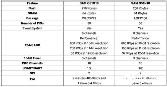
爱特梅尔SAM G51系列微控制器显示封装选择的范围:爱特梅尔SAM G51系列图2图像。该外设允许SAM G51系列针对广泛的应用,包括消费电子,工业控制和PC外设只有两种封装类型 - 一个49引脚WLCSP芯片级封装或100引脚LQFP封装。与此同时,Atmel的SAM4S系列也基于ARM Cortex-M4处理器核心。它工作在120 MHz的更高的最高速度,并设有高达2048 KB的闪存,可选双行执行与高速缓存,以及高达160字节的SRAM。外设集包括嵌入式收发器全速USB设备端口,高速MCI的SDIO / SD / MMC,内存控制器,两个USART,两个UART,二TWIs,三SPI的一I²S一个外部总线接口,还有一个PWM定时器,两个三通道通用的16位定时器(带步进电机和正交解码器逻辑支持),一个RTC,一个12位ADC,一个12位DAC和一个模拟比较器。所有这一切都使在包装和销数更大的要求。该系列有多达79 I /外部中断功能(边缘或水平灵敏度),消除抖动,假信号过滤和管芯串联电阻端接,以及三个32位并行输入/输出控制器O线。这导致了一系列的包,从100向下通往48引线,但使用更传统的技术:100引线封装
LQFP,14×14毫米,间距0.5毫米
TFBGA,9×9毫米,节距0.8毫米
VFBGA,7×7毫米,间距0.65毫米
64引脚封装
LQFP,10×10毫米,间距0.5毫米
QFN,9×9毫米,间距0.5毫米
WLCSP,4.42 x3.42毫米,间距0.4毫米(SAM4S16 / S8)
WLCSP,3.32 x3.32毫米,间距0.4毫米(SAM4S4 / S2)
48引脚封装
LQFP,7×7毫米,间距0.5毫米
QFN,7×7毫米,间距0.5毫米
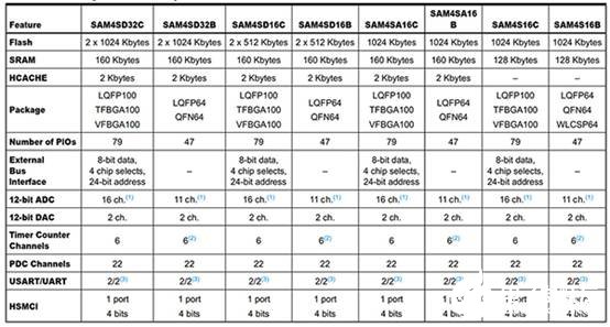
爱特梅尔SAM4S系列图3图片:爱特梅尔SAM4S系列具有更广泛的外设选项,导致更大的封装。未来趋势的新包装技术,堆叠死在彼此的顶部在同一个包也有利于降低整体的足迹。代替具有沿着微控制器单独的存储器芯片,该微控制器芯片被安装在一个封装的存储器芯片或大的FPGA的顶部。这种方法,通常称为2.5D,需要一个硅中介层,并通过硅通孔(TSV),这是一个相对较新的技术,现在是成熟和变得越来越普遍。这是用在那些需要大容量内存,不能有效的成本在单一芯片上集成的高端设备。全3D包装看到多个芯片堆叠直接在彼此顶部;或许与I /上边缘O垫,以允许不同的设备之间的互连。尽管这是一个长期的目标小型化,结合从微控制器的内存和无线接口印刷电路板的所有元素融入其中封装器件,它尚未攻克一批成本,可靠性和散热问题的。结论广泛来自多个供应商的微控制器隐藏在这种装置的小型化的策略。包装在不同的家庭从一个供应商的范围内,所有周围的相同的核心,显示足迹,外设组合,功率和系统尺寸之间的复杂的平衡。再往下的性能曲线,32位控制器具有复杂的外设,现在多一点几平方毫米以上,成为“硅尘”的渗透物联网。
 电子发烧友App







评论