 Linear Resistance Meter,线性刻度欧姆表

Linear Resistance Meter,线性刻度欧姆表
关键字:Linear Resistance Meter
Most analogue multimeters are capable of measuring resistance over quite a wide range of values, but are rather inconvenient in use due to the reverse reading scale which is also non-linear. This can also give poor accuracy due to cramping of the scale that occurs at the high value end of each range. This resistance meter has 5 ranges and it has a forward reading linear scale on each range.The full-scale values of the 5 ranges are 1K, 10K, 100K, 1M &10M respectively and the unit is therefore capable of reasonably accurate measurements from a few tens of ohms to ten Megohms.
Circuit diagram
The Circuit
Most linear scale resistance meters including the present design, work on the principle that if a resistance is fed from a constant current source the voltage developed across that resistance is proportional to its value. For example, if a 1K resistor is fed from a 1 mA current source from Ohm’s Law it can be calculated that 1 volt will be developed across the resistor (1000 Ohms divided by 0.001 amps = 1 volt). Using the same current and resistance values of 100 ohms & 10K gives voltages of 0.1volts (100 ohms / 0.001amps = 0.1volts) & 10 volts (10000 ohms / 0.001amps = 10 volts).
Thus the voltage developed across the resistor is indeed proportional to its value, and a voltmeter used to measure this voltage can in fact be calibrated in resistance, and will have the desired forward reading linear scale. One slight complication is that the voltmeter must not take a significant current or this will alter the current fed to the test resistor and impair linearity. It is therefore necessary to use a high impedance voltmeter circuit.
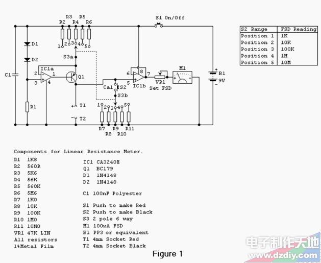
The full circuit diagram of the Linear Resistance Meter is given in Figure 1. The constant current generator is based on IC1a and Q1. R1, D1 and D2 form a simple form a simple voltage regulator circuit, which feeds a potential of just over 1.2 volts to the non-inverting input of IC1a. There is 100% negative feedback from the emitter of Q1 to the inverting input of IC1a so that Q1’s emitter is stabilised at the same potential as IC1a’s non-inverting input. In other words it is stabilised a little over 1.2 volts below the positive supply rail potential. S3a gives 5 switched emitter resistances for Q1, and therefore 5 switched emitter currents. S3b provides 5 reference resistors across T1 & T2 via S2 to set full-scale deflection on each range using VR1.
As the emitter and collector currents of a high gain transistor such as a BC179 device used in the Q1 are virtually identical, this also gives 5 switched collector currents. By having 5 output currents, and the current reduced by a factor of 10 each time S3a is moved one step in a clockwise direction, the 5 required measuring ranges are obtained. R2 to R6 must be close tolerance types to ensure good accuracy on all ranges. The high impedance voltmeter section uses IC1b with 100% negative feedback from the output to the inverting input so that there is unity voltage gain from the non-inverting input to the output. The output of IC1b drives a simple voltmeter circuit using VR1 and M1, and the former is adjusted to give the correct full-scale resistance values.
The CA3240E device used for IC1 is a dual op-amp having a MOS input stage and a class A output stage. These enable the device to operate with the inputs and outputs right down to the negative supply rail voltage. This is a very helpful feature in many circuits, including the present one as it enables a single supply rail to be used where a dual balanced supply would otherwise be needed. In many applications the negative supply is needed simply in order to permit the output of the op-amp to reach the 0volt rail. In applications of this type the CA3240E device normally enables the negative supply to be dispensed with.
As the CA3240E has a MOS input stage for each section the input impedance is very high (about 1.5 million Megohms!) and obviously no significant input current flows into the device. This, together with the high quality of the constant current source, and the practically non-existent distortion through IC1b due to the high feedback level gives this circuit excellent linearity.
With no resistor connected across T1 & T2 M1 will be taken beyond full-scale deflection and overloaded by about 100 or 200%. This is unlikely to damage the meter, but to be on the safe side a push-to-test on/off switch (S1) is used. Thus the power is only applied to the circuit when a test resistor is connected to the unit, and prolonged meter overloads are thus avoided.
A small (PP3 size) 9 volt battery is a suitable power source for this project which has a current consumption of around 5mA and does not require a stabilised supply.
Most linear scale resistance meters including the present design, work on the principle that if a resistance is fed from a constant current source the voltage developed across that resistance is proportional to its value. For example, if a 1K resistor is fed from a 1 mA current source from Ohm’s Law it can be calculated that 1 volt will be developed across the resistor (1000 Ohms divided by 0.001 amps = 1 volt). Using the same current and resistance values of 100 ohms & 10K gives voltages of 0.1volts (100 ohms / 0.001amps = 0.1volts) & 10 volts (10000 ohms / 0.001amps = 10 volts).
Thus the voltage developed across the resistor is indeed proportional to its value, and a voltmeter used to measure this voltage can in fact be calibrated in resistance, and will have the desired forward reading linear scale. One slight complication is that the voltmeter must not take a significant current or this will alter the current fed to the test resistor and impair linearity. It is therefore necessary to use a high impedance voltmeter circuit.
The full circuit diagram of the Linear Resistance Meter is given in Figure 1. The constant current generator is based on IC1a and Q1. R1, D1 and D2 form a simple form a simple voltage regulator circuit, which feeds a potential of just over 1.2 volts to the non-inverting input of IC1a. There is 100% negative feedback from the emitter of Q1 to the inverting input of IC1a so that Q1’s emitter is stabilised at the same potential as IC1a’s non-inverting input. In other words it is stabilised a little over 1.2 volts below the positive supply rail potential. S3a gives 5 switched emitter resistances for Q1, and therefore 5 switched emitter currents. S3b provides 5 reference resistors across T1 & T2 via S2 to set full-scale deflection on each range using VR1.
As the emitter and collector currents of a high gain transistor such as a BC179 device used in the Q1 are virtually identical, this also gives 5 switched collector currents. By having 5 output currents, and the current reduced by a factor of 10 each time S3a is moved one step in a clockwise direction, the 5 required measuring ranges are obtained. R2 to R6 must be close tolerance types to ensure good accuracy on all ranges. The high impedance voltmeter section uses IC1b with 100% negative feedback from the output to the inverting input so that there is unity voltage gain from the non-inverting input to the output. The output of IC1b drives a simple voltmeter circuit using VR1 and M1, and the former is adjusted to give the correct full-scale resistance values.
The CA3240E device used for IC1 is a dual op-amp having a MOS input stage and a class A output stage. These enable the device to operate with the inputs and outputs right down to the negative supply rail voltage. This is a very helpful feature in many circuits, including the present one as it enables a single supply rail to be used where a dual balanced supply would otherwise be needed. In many applications the negative supply is needed simply in order to permit the output of the op-amp to reach the 0volt rail. In applications of this type the CA3240E device normally enables the negative supply to be dispensed with.
As the CA3240E has a MOS input stage for each section the input impedance is very high (about 1.5 million Megohms!) and obviously no significant input current flows into the device. This, together with the high quality of the constant current source, and the practically non-existent distortion through IC1b due to the high feedback level gives this circuit excellent linearity.
With no resistor connected across T1 & T2 M1 will be taken beyond full-scale deflection and overloaded by about 100 or 200%. This is unlikely to damage the meter, but to be on the safe side a push-to-test on/off switch (S1) is used. Thus the power is only applied to the circuit when a test resistor is connected to the unit, and prolonged meter overloads are thus avoided.
A small (PP3 size) 9 volt battery is a suitable power source for this project which has a current consumption of around 5mA and does not require a stabilised supply.
Photos showing inside and outside of the completed Linear Resistance Meter.
Author: Dave Elliott
Email: portagepal@tiscali.co.uk
Email: portagepal@tiscali.co.uk
声明:本文内容及配图由入驻作者撰写或者入驻合作网站授权转载。文章观点仅代表作者本人,不代表电子发烧友网立场。文章及其配图仅供工程师学习之用,如有内容侵权或者其他违规问题,请联系本站处理。
举报投诉
发布评论请先 登录
相关推荐
热点推荐
BNC接头50欧姆与75欧姆外观几乎一样?一个实测波形告诉你差别在哪
外观几乎一致的50欧姆与75欧姆BNC接头,混用会有什么后果?本文通过TDR阻抗曲线和眼图等实测波形,直观展示了阻抗失配带来的信号反射、过冲及振铃畸变。文章深入剖析了由中心针径与特氟龙介质分布引起的物理根源,并分享了实用的选型防错经验,助您保障工业级高频链路的阻抗稳定性。

BNC连接器选型时别只看价格不看规格!50欧姆和75欧姆混用后果实测
文章深度剖析了 50 欧姆与 75 欧姆 BNC 在中心针、特氟龙介质等物理结构上的本质区别,并结合 德索连接器(Dosin) 实验室的实测数据,揭示了混插导致结构破坏、高频阻抗失配等致命后果。文中

S32K396 eFlexPWM如何配置PWM周期和占空比的刻度
,无需 CPU 干预
运行时职责更新:
占空比可能会在运行时发生变化。必须进行更新仅在重新加载事件中以防止输出故障。
需要澄清:
如何配置PWM周期和占空比的刻度
哪VALx 事件是否建议在中心对齐
发表于 05-14 06:12
欧姆定律电压与电流及电阻之间的关系
欧姆定律是电路的基本原理,用“电流=电压÷电阻”的公式来表述电流、电压与电阻三者之间的关系。电压越高电流越大,而电阻越大则电流越小。例如,在将干电池与灯泡串联连接的电路中,电池的电压和灯泡的电阻共同

深入解析TSS721A:Meter - Bus标准的高效收发器
深入解析TSS721A:Meter - Bus标准的高效收发器 在电子设备通讯领域,Meter - Bus标准应用广泛,德州仪器(TI)的TSS721A单芯片收发器就是为Meter - Bus标准
TSS521 Meter-Bus 收发器:技术解析与应用指南
TSS521 Meter-Bus 收发器:技术解析与应用指南 在电子工程领域,Meter-Bus 标准的应用十分广泛,它为智能计量设备的通信提供了可靠的解决方案。TI 公司的 TSS521 单芯片
探索Bourns MT系列低欧姆功率电阻:特性、规格与应用考量
探索Bourns MT系列低欧姆功率电阻:特性、规格与应用考量 在电子设计领域,电阻作为基础电子元件,其性能对电路的稳定性和可靠性起着关键作用。今天我们要深入探讨的是Bourns的MT系列
探索OPTIREG™ Linear TLS850C2TEVxx Demoboard:低功耗线性稳压器的理想之选
探索OPTIREG™ Linear TLS850C2TEVxx Demoboard:低功耗线性稳压器的理想之选 在电子工程师的日常工作中,寻找性能卓越、稳定性高且适用于多种场景的电压调节器至关重要
OPTIREG™ Linear TLS850C2TEVxx Demoboard:低功耗线性稳压器的理想之选
OPTIREG™ Linear TLS850C2TEVxx Demoboard:低功耗线性稳压器的理想之选 在电子设计领域,电压调节器是至关重要的组件,它能为电子设备提供稳定的电源,确保设备正常运行
OptiMOS™ 5 Linear FET 2, 100 V IPT017N10NM5LF2 MOSFET深度解析
OptiMOS™ 5 Linear FET 2, 100 V IPT017N10NM5LF2 MOSFET深度解析 作为电子工程师,我们在设计中常常需要挑选合适的MOSFET来满足特定的应用需求
线性搜索与二分搜索介绍
线性搜索(Linear Search):从数组的第一个元素开始,依次将当前元素与目标值进行比较,直到找到目标值或搜索完整个数组。
二分搜索(Binary Search):在有序数组中查找某一特定元素
发表于 12-01 07:36
欧姆龙多款检测设备亮相NEPCON ASIA 2025
在即将开展的NEPCON ASIA 2025上,作为连续十余年参展NEPCON ASIA的自动化领军企业和检测行业专家,欧姆龙自动化(中国)有限公司(以下简称“欧姆龙”)将带来多款高性能检测设备,覆盖X射线检查、外观AOI及锡膏印刷检测等关键工艺环节,为电子制造提供全面质
50 欧姆、高 IP3、低噪声宽带增益模块 skyworksinc
IP3、低噪声宽带增益模块真值表,50 欧姆、高 IP3、低噪声宽带增益模块管脚等资料,希望可以帮助到广大的电子工程师们。
发表于 09-01 18:32

线性放大器 skyworksinc
电子发烧友网为你提供()线性放大器相关产品参数、数据手册,更有线性放大器的引脚图、接线图、封装手册、中文资料、英文资料,线性放大器真值表,线性
发表于 09-01 18:31
用数字万用表判断常用电子元器件
并联的分流电阻随量程的增大,其阻值几乎10倍的增加,A、B两点的电压也会逐次增大,流过表头的电流也增大,表针偏转超过满刻度,因此在改变量程时要调零。所以当万用表置各量程时,回路的电流是不同的。
量程
发表于 05-27 16:03


评论