ADI公司的ADMV4420是集成了分数-N PLL和VCO的K波段下变换器,具有高度集成双平衡有源混频器和分数N合成器,其RF前端包括集成的平衡/不平衡变换器(balun)和低噪音放大器(LNA)(7dB单边带噪音),以及高动态范围IF输出放大器,其转换增益36dB.集成的低相位噪音分数N锁相环(PLL)和多核压控振荡器(VCO)和内部2x乘法器,输出P1dB为7 dBm,输出IP3为16 dBm,RF输入频率16.95 GHz 到 22.05 GHz, LO频率范围16.75 GHz to 21.15 GHz, IF频率范围900 MHz 到 2500 MHz ,5V工作电压,主要用在卫星通信和点对点微波通信。本文介绍了ADMV4420主要特性,功能框图以及评估板ADMV4420-EVALZ主要特性,配置图和实验室连接图,电路图,材料清单和PCB设计图。
The ADMV4420 is a highly integrated, double balanced, active mixer with an integrated fractional-N synthesizer, ideally suited for next generation K band satellite communications.
The RF front end consists of an integrated RF balun and low noise amplifier (LNA) for an optimal, 7 dB, single-sideband noise figure while minimizing external components. Additionally, the high dynamic range IF output amplifier provides a nominal conversion gain of 36 dB.
An integrated low phase noise, fractional-N, phase-locked loop (PLL) with a multicore voltage controlled oscillator (VCO) and internal 2× multiplier generate the necessary on-chip LO signal for the double balanced mixer, eliminating the need for external frequency synthesis. The multicore VCO uses an internal autocalibration routine that allows the PLL to select the necessary settings and lock in approximately 400 μs.
The reference input to the PLL employs a differentially excited 50 MHz crystal oscillator. Alternatively, the reference input can be driven by an external, singled-ended, 50 MHz source. The phase frequency detector (PFD) comparison frequency of the PLL operates up to 50 MHz.
The ADMV4420 is fabricated on a silicon germanium (SiGe), bipolar complementary metal-oxide semiconductor (BiCMOS) process, and is available in a 32-lead, RoHS compliant, 5 mm × 5 mm LFCSP package with an exposed pad. The device is specified over the −40°C to +85°C temperature range on a 5 V power supply.
ADMV4420主要特性:
RF front end with integrated RF balun and LNA
Double balanced, active mixer with high dynamic range IF amplifier
Fractional-N synthesizer with low phase noise, multicore VCO
5 V supply operation with integrated LDO regulators
Output P1dB: 7 dBm
Output IP3: 16 dBm
Conversion gain: 36 dB
Noise figure: 7 dB
RF input frequency range: 16.95 GHz to 22.05 GHz
Internal LO frequency range: 16.75 GHz to 21.15 GHz
IF frequency range: 900 MHz to 2500 MHz
Single-ended 50 Ω input impedance and 75 Ω IF output impedance
Programmable via 4-wire SPI
32-lead, 5 mm × 5 mm LFCSP
ADMV4420应用:
Satellite communication
Point to point microwave communication
![[原创]ADI ADMV4420 K波段下变换器解决方案](/uploads/allimg/181116/1513024V6_0.png)
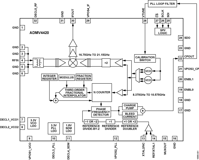
图1. ADMV4420功能框图
评估板ADMV4420-EVALZ
The ADMV4420-EVALZ evaluation board can be used to evaluate the performance of the ADMV4420. The top and cross sectional layout views of the ADMV4420-EVALZ evaluation board are shown in Figure 126 and Figure 127, respectively. The RF transmission lines were designed using a coplanar waveguide (CPWG) model with a line width (W) of 16 mil and 13 mil of ground spacing for a characteristic impedance of 50Ω for the RF input (RFIN) and the external reference input (REF/XTAL1)。 The line width and ground spacing for the IF output (IFOUT) are 9 mil and 15 mil, respectively. The PCB is made with Rogers 4350B dielectric material, which offers low loss performance, and isola 370HR dielectric material, which achieves the required thickness of the PCB.
The ADMV4420-EVALZ comes with an ADMV4420 chip. Figure 4 shows the location of this chip on the evaluation board and the block diagram of the ADMV4420.
When evaluating the device, connect the RF input to an RF signal generator. The ADMV4420-EVALZ runs on a 5 V dc supply. Figure 2 shows the top side of the ADMV4420-EVALZ and is intended for evaluation purposes only.
Connect the 5 V dc to the VPOS1 test point and ground to the GND2 test point on the ADMV4420-EVALZ. Connect a 50 Ω SMA female to a 75 Ω Type F male adapter to J4 (IF output)。 Connect the output of the adapter to a spectrum analyzer. The ADMV4420-EVALZ has 50 MHz crystal on board. Optionally, the user can connect a reference signal from a low phase signal generator to the J2 SMA connector. If the user wants to use an external reference, depopulate Y1, C5, and C6 and then install a 0.01 μF capacitor at C21, a 1 nF capacitor at C6, and 50 Ω at R21. See Figure 5 for ADMV4420-EVALZ lab connections. Figure 3 shows the block diagram of the ADMV4420 lab bench setup.
评估板ADMV4420-EVALZ主要特性:
Full feature evaluation board for the ADMV4420
On-board SDP-S connector for SPI control
5 V operation
ACE software interface for SPI control
图2. 评估板ADMV4420-EVALZ外形图
![[原创]ADI ADMV4420 K波段下变换器解决方案](/uploads/allimg/181116/1515025625_0.png)
图3. 评估板ADMV4420-EVALZ电路图
评估板ADMV4420-EVALZ材料清单:
![[原创]ADI ADMV4420 K波段下变换器解决方案](/uploads/allimg/181116/1516011545_0.png)
![[原创]ADI ADMV4420 K波段下变换器解决方案](/uploads/allimg/181116/151F1Jb_0.png)
![[原创]ADI ADMV4420 K波段下变换器解决方案](/uploads/allimg/181116/151P1P60_0.png)
图4. 评估板ADMV4420-EVALZ配置图
![[原创]ADI ADMV4420 K波段下变换器解决方案](/uploads/allimg/181116/151Z2EH_0.png)
图5. 评估板ADMV4420-EVALZ实验室连接图
![[原创]ADI ADMV4420 K波段下变换器解决方案](/uploads/allimg/181116/15200262C_0.png)
图6. 评估板ADMV4420-EVALZ 18GHz RF信号,17GHz LO和50MHz板上晶振设定图
![[原创]ADI ADMV4420 K波段下变换器解决方案](/uploads/allimg/181116/1521022353_0.png)
图7. 评估板ADMV4420-EVALZ 18GHz RF信号,20.2GHz LO和50MHz板上晶振设定图
图8. 评估板ADMV4420-EVALZ 顶视图
图9. 评估板ADMV4420-EVALZ 底视图
图10. 评估板ADMV4420-EVALZ PCB顶视图
图11. 评估板ADMV4420-EVALZ实验室工作台建立框图
![[原创]ADI ADMV4420 K波段下变换器解决方案](/uploads/allimg/181116/1526014952_0.png)
图12. 评估板ADMV4420-EVALZ 布局图(顶视图1)
![[原创]ADI ADMV4420 K波段下变换器解决方案](/uploads/allimg/181116/152F14931_0.png)
图12. 评估板ADMV4420-EVALZ 布局图(层2)
![[原创]ADI ADMV4420 K波段下变换器解决方案](/uploads/allimg/181116/152P2O28_0.png)
图13. 评估板ADMV4420-EVALZ 布局图(层3)
![[原创]ADI ADMV4420 K波段下变换器解决方案](/uploads/allimg/181116/152Z2a64_0.png)
图14. 评估板ADMV4420-EVALZ 布局图层4(底面)
详情请见:
https://www.analog.com/media/en/technical-documentation/data-sheets/ADMV4420.pdf
和
https://www.analog.com/media/en/technical-documentation/user-guides/ADMV4420-EVALZ-UG-1404.pdf
ADMV4420.pdf
ADMV4420-EVALZ-UG-1404.pdf
-
变换器
+关注
关注
17文章
2096浏览量
109250 -
RF
+关注
关注
65文章
3046浏览量
166948
发布评论请先 登录
相关推荐
贸泽开售Analog Devices用于卫星通信的 ADMV4540 K波段正交解调器

DC-DC变换器解决方案
双波段阻抗变换器
用DC/DC变换器的高效电源解决方案

ADMV4420 具有集成小数 N 分频 PLL 和 VCO 的 K 波段下变频器

UG-1404:评估集成小数N锁相环和压控振荡器的ADMV4420,K波段下变频器


 ADMV4420的K波段下变换器解决方案


评论