nxp公司的QN9080-001-M17是支持BLE和NFC的超小型预先认证蓝牙5.0 MCU,集成了NFC NTAG®连接性。超小型器件是基于QN9080芯片和NT3H2211芯片。而QN9080芯片是基于Arm Cortex-M4F MCU,具有专用融合传感器协处理器(FSP),由于对硬件卸载了复杂数学算法而进一步降低功耗; NT3H2211芯片是具有I2C接口的NFC Forum Type 2 Tag兼容的IC,提供了最快最便宜方式以增加感应式(tap and go)连接性。 QN9080-001-M17还集成32MHz和32.768 kHz晶体,2.4GHz优化天线和运行QN9080系统所需要的必备的元件,集成了512KB闪存,128KB RAM,提供了需要BLE无线连接以及快速和NTAG配对的完整解决方案。它的外接元件数量少能降低系统尺寸,复杂性和缩短开发时间。发送功率高达+2dBm,接收灵敏度-92.7dBm(1Mbps模式)和-89dBm(2Mbps模式),主要用在健康和医疗设备,运动和健美跟踪器,建筑物和家庭自动化,零售和广告信标。本文介绍了QN9080SIP主要特性和优势,QN9080主要特性以NTAG主要特性与集成2.4GHz天线主要特性,以及QN9080-001-M17-高级HW框图,QN9080-001-M17评估板QN9080DK主要特性,电路图和PCB设计图。
The QN9080-001-M17 is a fully certified device supporting BLE and NFC. It has ultra-low power consumption, highly integrated with rich feature sets, fully FCC/CE/IC/MIC certified. The QN9080-001-M17 supports Bluetooth 5, and it is intended for ultra-small, portable connected wireless applications.
This ultra-small device is based on QN9080 die and NT3H2211 die. QN9080 is powered by an Arm Cortex-M4F, and has a dedicated fusion sensor co-processor (FSP) to further reduce power consumption by off-loading complex math computations to the hardware. 512 KB of on-board flash and 128 KB SRAM provide enough room and flexibility for complex applications. NT3H2211 is NFC Forum Type 2 Tag compliant IC with I2C interface, which supplies the fastest, least expensive way to add tap-and-go connectivity to just about any electronic applications.
The QN9080-001-M17 also integrates 32 MHz and 32.768 kHz crystals, a 2.4 GHz optimized antenna, and necessary components for QN9080 system to run. It offers a complete solution for applications requiring BLE wireless connectivity and fast pairing with NTAG as an option. Its low external component count reduces overall system size,complexity and shortens development time.
QN9080SIP主要特性和优势:
主要特性:
Bluetooth 5.0 certified
Integrated antenna
Integrated 32 MHz and 32.768 kHz crystals
32-bit Arm Cortex-M4F core at 32 MHz
512 KB flash
128 KB RAM
TX power: up to +2 dBm
RX sensitivity: -92.7 dBm in 1 Mbps mode and -89 dBm in 2 Mbps mode
True single-chip Bluetooth Low Energy (v5.0) SoC solution:
Integrated Bluetooth LE radio, protocol stack and application profiles
Support central and peripherals roles
Support master/slave concurrency
Support 16 simultaneous links
Support secure connections
Support data packet length extension
48-bit unique BD address
-92.7 dBm in 1 Mbps mode and -89 dBm in 2 Mbps mode
TX output power from -20 dBm to +2 dBm
Very low power consumption:
Single 1.67 V ~3.6 V power supply
1 A power-down mode, to wake up by GPIO
2 A power-down mode, to wake up by 32 kHz sleep timer, RTC and GPIO
4 mA RX current at 3 V supply in 1 Mbps
Ultra Low power Bluetooth Low Energy 5.0 module
3.5 mA TX current at 0 dBm TX power at 3 V supply in 1 Mbps mode
Interface:
32 General-Purpose Input/Output (GPIO) pins, with configurable pull-up/pull-down
resistors
8 external ADC inputs (shared with GPIO pins)
2 Analog Comparator input pins (share with GPIO pins)
Single power supply 1.67 V to 3.6 V
Operating temperature range -40℃ to +85℃
6 x9.7x1.17 mm LFLGA package
QN9080主要特性:
True single-chip Bluetooth Low Energy (v5.0) SoC solution
Integrated Bluetooth LE radio, protocol stack and application profiles
Supports central and peripherals roles
Supports master/slave concurrency
Supports 16 simultaneous links
Supports secure connections
Supports data packet length extension
Wifi/Bluetooth LE coexistence interface
48-bit unique bluetooth device address
RF
Fast and reliable RSSI in 1 dB step
TX output power from 20 dBm to 2 dBm
Single-ended RF port with integrated balun
Generic FSK modulation with programmed data rate from 250 Kbps to 2 Mbps
Compatible with worldwide radio frequency regulations
Very low power consumption
Single 1.67 V to 3.6 V power supply
Integrated DC-to-DC buck converter and LDO
1.0 A power-down 1 mode, to wake up by GPIO
2.5 A power-down 0 mode, to wake up by 32 kHz sleep timer, RTC and GPIO
3.5 mA RX current with DC-to-DC convertor enabled at 3 V supply in 1Mbps mode
4 mA TX current at 0 dBm TX power with DC-to-DC converter enabled at 3 Vsupply in 1 Mbps mode
Arm Cortex-M4 core (version r0p1)
Arm Cortex-M4 processor, running at a frequency of up to 32 MHz
Floating Point Unit (FPU) and Memory Protection Unit (MPU)
Arm Cortex-M4 built-in Nested Vectored Interrupt Controller (NVIC)
Serial Wire Debug (SWD) with six instruction breakpoints, two literal comparators,and four watch points, including serial wire output for enhanced debug capabilities
System tick timer
On-chip memory
512 KB on-chip flash program memory and 2 KB page erase and write
128 KB SRAM
256 KB ROM
ROM API support
Flash In-System Programming (ISP)
Serial interfaces
Four Flexcomm serial peripherals
USART protocol supported by Flexcomm0, USART and I2C by Flexcomm1, SPIand I2C by Flexcomm2, and SPI by Flexcomm3
Each Flexcomm includes a FIFO
I2C-bus interfaces support fast mode and with multiple address recognition andmonitor mode
USB 2.0 (full speed) device interface
Two quadrature decoders
SPI Flash Interface (SPIFI) uses a SPI bus superset with four data lines to access
off-chip quad SPI flash memory at a much higher rate than is possible usingstandard SPI or SSP interfaces
Supports SPI memories with 1 or 4 data lines
Digital peripherals
DMA controller with 20 channels, able to access memories and DMA capable
peripherals
Up to 35 General Purpose Input Output (GPIO) pins, with configurable pull-up or
pull-down resistors
GPIO registers are located on the AHB for fast access
32 GPIOs can be selected as Pin INTerrupts (PINT), triggered by rising, or falling
input edges
AES-128 security coprocessor
Random Number Generator (RNG)
CRC engine
Fusion Signal Processor (FSP) for data fusion and machine learning algorithms
resulting in low power consumption compared to software processing
Analog peripherals
16-bit ADC with 8 external input channels, with sample rates of up to 32k sample
per second, and with multiple internal and external trigger inputs
Integrated temperature sensor, connected to one internal dedicated ADC channel
Integrated battery monitor connected to one internal dedicated ADC channel
General-purpose 8-bit 1M sample per second DAC
Integrated capacitive sense up to 8 channels, able to wake up the MCU from low
power states.
Twoultra low-power analog comparators, able to wake up the MCU from low power
states.
Timers
Four 32-bit general-purpose timers or counters, support capture inputs and
compare outputs, PWM mode, and external count input
Sleep timer, which can work in power-down mode and wake up MCU
32-bit Real Time Clock (RTC) with 1 second resolution running in the always-on
power domain; can be used for wake-up from all low power modes includingpower-down
Watchdog Timer.
SC Timer or PWM.
Clock generation
32 MHz internal RC oscillator, which can be used as a system clock
16 MHz or 32 MHz crystal oscillator, which can be used as a system and RFreference
32 kHz on-chip RC oscillator
32.768 kHz crystal oscillator
Power control
Programmable Power Management Unit (PMU) to minimize power consumption
Reduced power modes: sleep, and power-down
Power-On Reset (POR)
Brown-Out Detection (BOD) with separate thresholds for interrupt and forced reset
Single power supply 1.67 V to 3.6 V
Operating temperature range 40 ℃ to +85 ℃
NTAG主要特性:
Interoperability
ISO/IEC 14443 Part 2 and 3 compliant
NTAG I2C plus development board is certified as NFC Forum Type 2 Tag
(Certification ID: 58514)
Unique 7-byte UID
GET_VERSION command for easy identification of chip type and supportedfeatures
Input capacitance of 50 pF
Host interface
I2C slave
Configurable event detection pin to signal NFC or pass-through data events
Memory
1912 bytes of EEPROM-based user memory
64 bytes SRAM buffer for transfer of data between NFC and I2C interfaces withmemory mirror or pass-through mode
Clear arbitration between NFC and I2C memory access
Data transfer
Pass-through mode with 64-byte SRAM buffer
FAST_WRITE and FAST_READ NFC commands for higher data throughput
Security and memory-access management
Full, read-only, or no memory access from NFC interface, based on 32-bit
password
Full, read-only, or no memory access from I2C interface
NFC silence feature to disable the NFC interface
Originality signature based on Elliptic Curve Cryptography (ECC) for simple,
genuine authentication
Power Management
Configurable field-detection output signal for data-transfer synchronization and
device wake-up
Energy harvesting from NFC field, so as to power external devices (e.g. connected
microcontroller)
集成2.4GHz天线主要特性:
Monolithic SMD with small, low-profile and light-weight type.
Wide bandwidth
RoHS compliant
QN9080SIP应用:
Health and medical devices
Sports and fitness trackers
Building and home automation
Retail and advertising beacons

图1.QN9080-001-M17-高级HW框图

图2.采用外接天线的QN9080-001-M17框图
QN9080-001-M17目标应用:
Consumer Electronics
Consumers and wearables
QN9080-001-M17评估板QN9080DK
The QN9080DK board is designed to make it as easy as possible to get started with your project based on NXP® QN908x BLE SOC. The QN9080DK board integrates buttons, Piezo buzzer, LED for easy way to reset chip and indicate chip status. The DK board also provides useful interfaces such as USB port for UART communication and CMSIS-DAP debug.
The QN9080-001-M17 DK board is designed to ease the evaluation of the chip ’ s functions and performance on customer side to make it easy to control, connect, and debug the extension hardware and make it easy for the customer to develop and debug firmware.
The QN9080-001-M17 DK board provides easy access to peripherals, such as buttons and LEDs. The board also provides useful interfaces, such as the USB port for UART communication, the CMSIS-DAP debugger, and the standard Arduino and Pmod connector. The USB dongle is a Bluetooth® device powered by QN9080. It acts as a master/slave when communicating with QN9080-001-M17 devices.
图3.评估板QN9080DK外形图

图4.评估板QN9080DK电源电路图
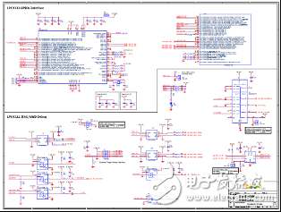
图5.评估板QN9080DK LPC处理器电路图

图6.评估板QN9080DK QN908x-BLE电路图

图7.评估板QN9080DK QN908x功能电路图
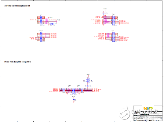
图8.评估板QN9080DK Arduino接口电路图
QN9080-001-M17模块板
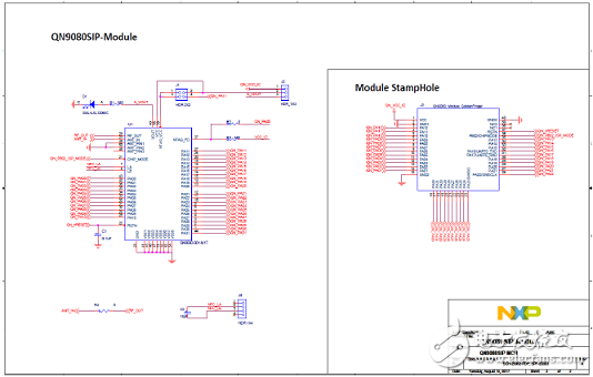
图9.QN9080-001-M17模块板电路图
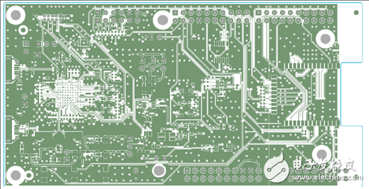
图10.QN9080-001-M17 DK主板PCB设计图:顶层腐蚀图
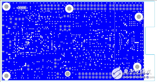
图11.QN9080-001-M17 DK主板PCB设计图:GND平面

图12.QN9080-001-M17 DK主板PCB设计图:PWR平面
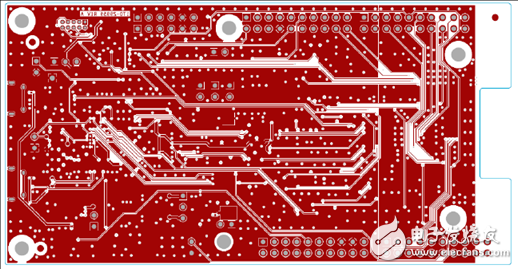
图12.QN9080-001-M17 DK主板PCB设计图:底层腐蚀图

图12.QN9080-001-M17 DK主板PCB设计图:顶层丝印图
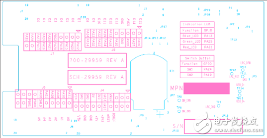
图13.QN9080-001-M17 DK主板PCB设计图:底层丝印图

图14.QN9080-001-M17板PCB设计图:顶层腐蚀图

图15.QN9080-001-M17板PCB设计图:GND平面

图16.QN9080-001-M17板PCB设计图:PWR平面

图17.QN9080-001-M17板PCB设计图:底层腐蚀图
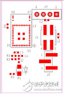
图18.QN9080-001-M17板PCB设计图:顶层丝印图
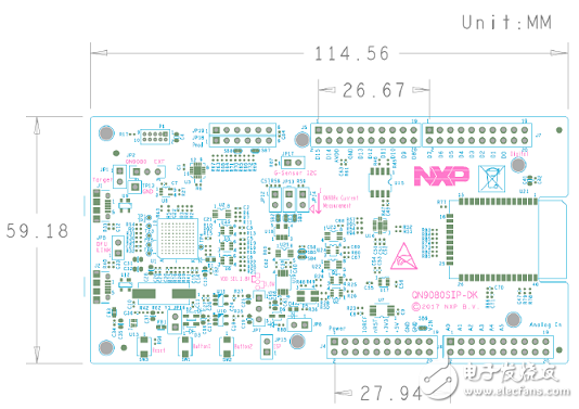
图19.QN9080-001-M17模块PCB设计图
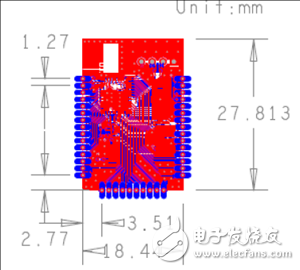
图20.QN9080-001-M17模块板尺寸图

图21.QN9080-001-M17 DK板上的锂电池
-
mcu
+关注
关注
146文章
17316浏览量
352442 -
蓝牙5.0
+关注
关注
9文章
88浏览量
28027
发布评论请先 登录
相关推荐
大联大世平集团推出基于NXP产品的多功能低功耗蓝牙电子锁方案
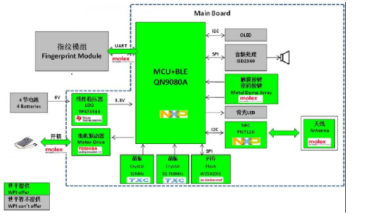


 基于QN9080SIP的低功耗蓝牙5.0MCU的解决方案


评论