电路能力测试-3:影像信号放大电路
Circuit Knowledge Test-3: Video Buffer

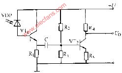
1. If video input voltage is 1 Vpp, what will be video voltage at QV2 collector and QV1 collector? (Line output with or without 75 ohm load)
影像信号输入为1V峰对峰值,计算QV2及QV1集极信号电压值。(包括输出端有无75 Ohm负载)
2. How to check video output waveform in order to make sure the video buffer circuit is working properly? (Hint: most common happened clamped video and tilted sync defects)
如何以仪器确认影像信号经过放大以后,输出波形为正常。(一般会有上下波幅切割或是同步信号扭曲问题)
3. Which components are needed to be value-changed for the adjustments of QV1 and QV2 collector bias? How to adjust for top side or bottom side clamped video?
那些元件是用来调整QV2及QV1的集极电压,以避免输出信号的上下切割问题。问题发生时,元件数值应该如何改变处理。
4. Plot the waveform for a regular pulse and pulses on
绘出下列五种波形:标准脉波,低频不足的脉波,高频不足的脉波,过冲震荡脉波,下冲震荡脉波。
试题解答
Circuit Knowledge Test-3: Video Buffer
ANS-1:
Buffer gain Av for QV2 = RV4/RV7 = 1.8
Buffer gain Av for QV1 = RV9/RV2 = 1.8 (without 75 Ohm load)
While QV2 load will change to 43 Ohm with 75 Ohm load. RV9/RV2 = 0.8
Video voltage at QV2 is 1.8 Vpp, at QV1 is 3.2 Vpp without load and 1.4 Vpp with load.
ANS-2:
Utilize gray scale pattern video signal with H-sync sweep scope setting to check clamped video defect.
Correct percentage of sync level must be 30% to show no clamped video defect.
Utilize full white pattern video signal with V-sync sweep scope setting to check tilted sync defect.
No tilted V-sync pulse and no tilted peak white are allowed.
ANS-3:
RV3 is suitable for adjusting QV2 bias, while RV8 is suitable for adjusting QV1 bias.
Increase RV3 value or reduce RV8 value for modified bottom side clamped video.
Reduce RV3 value or increase RV8 value for modified top side clamped video.
ANS-4:

 电子发烧友App









评论