反相放大器 The Inverting Amplifier
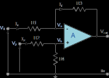
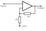
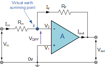
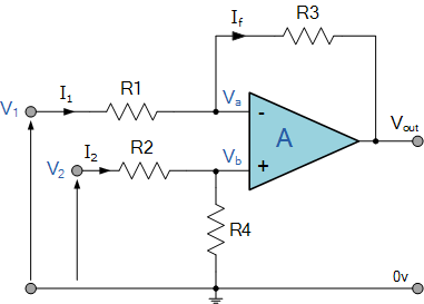
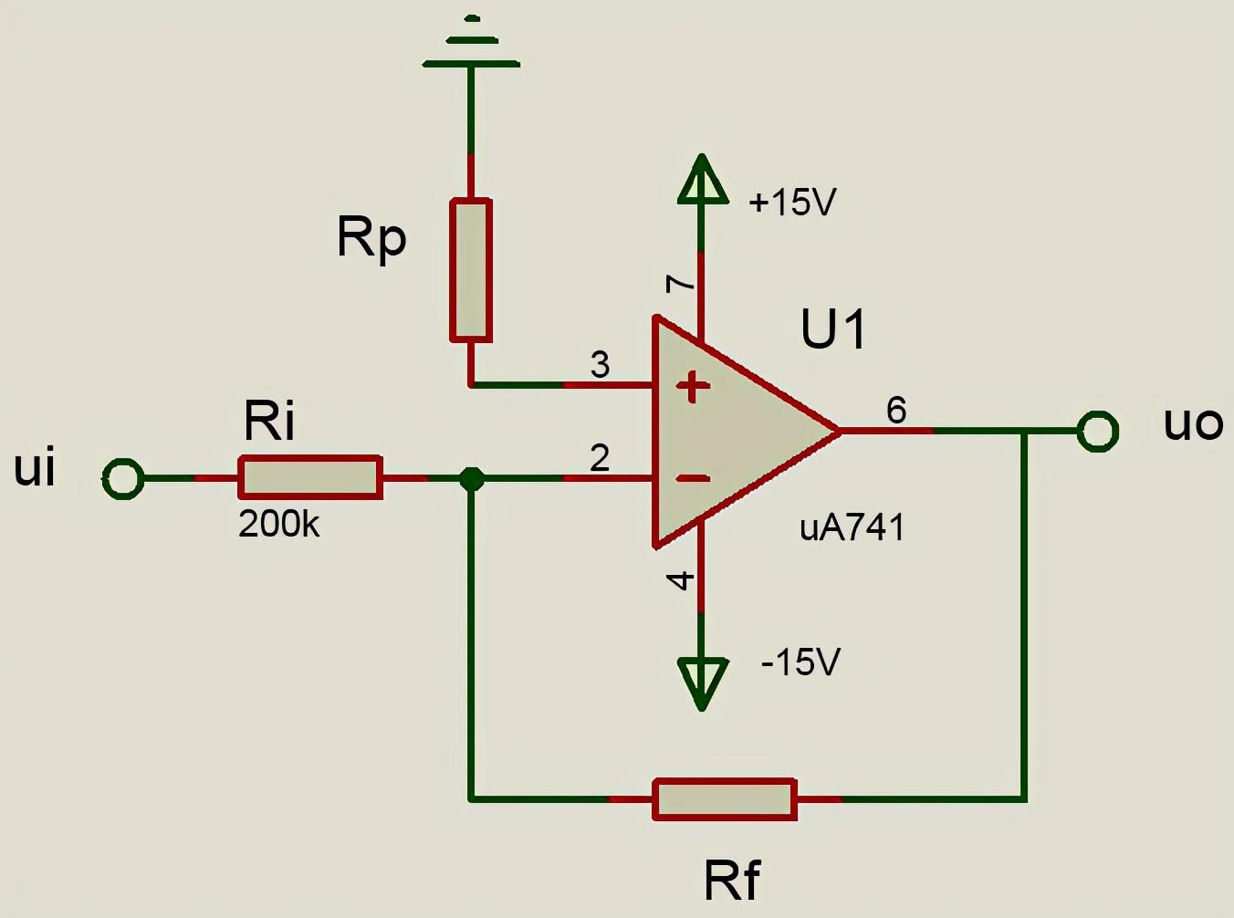
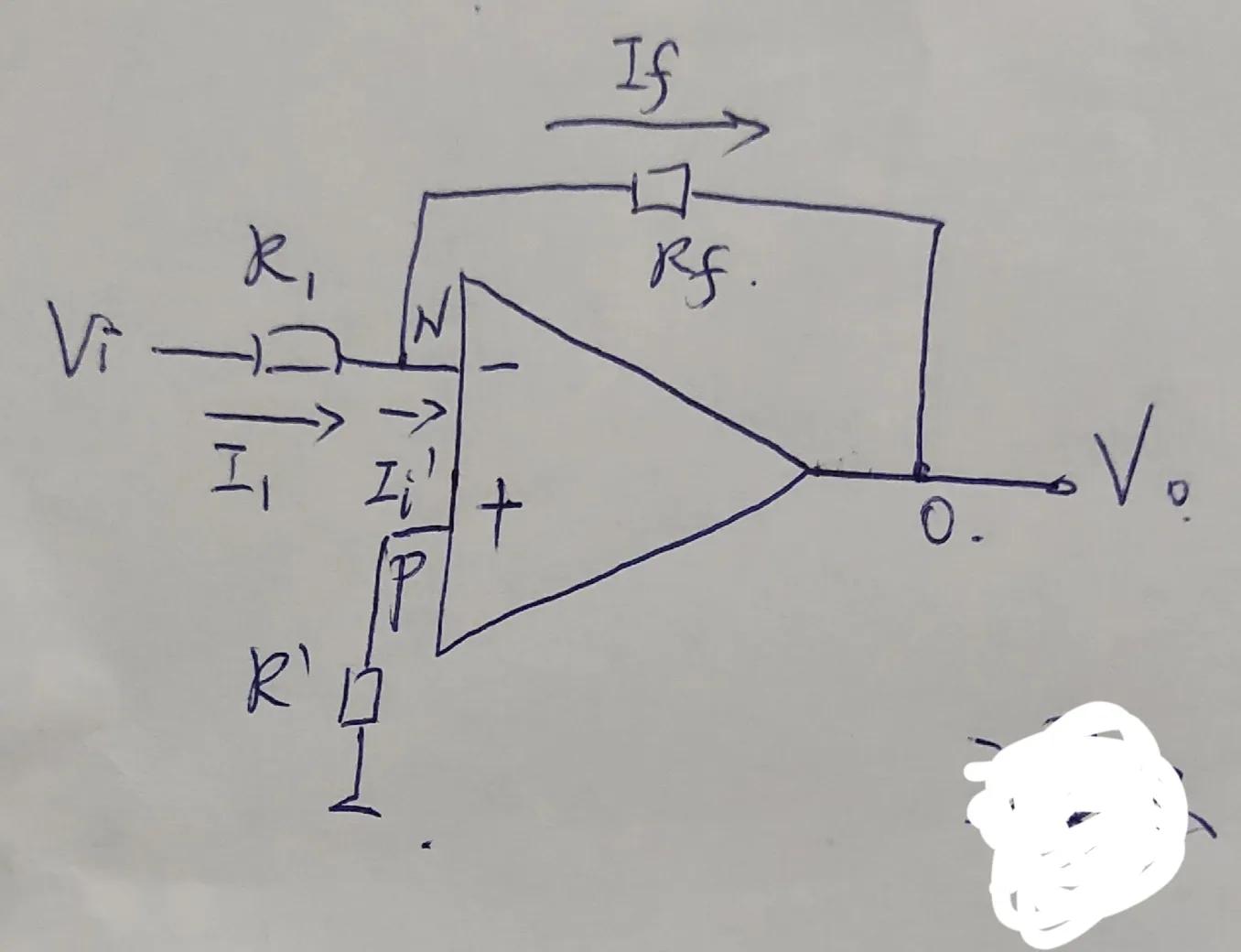
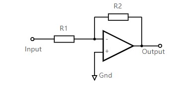
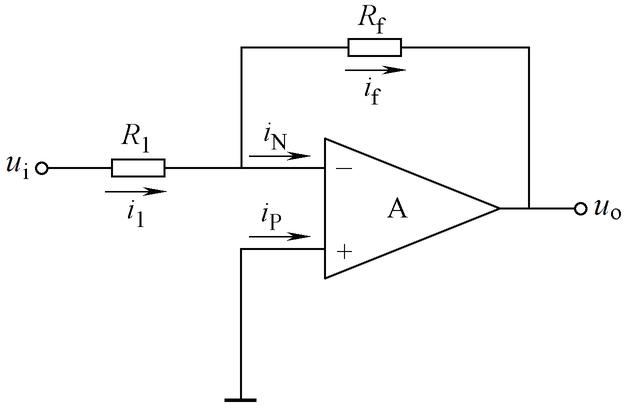
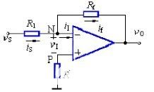
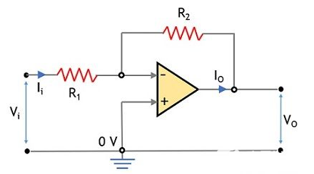
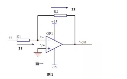
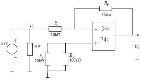
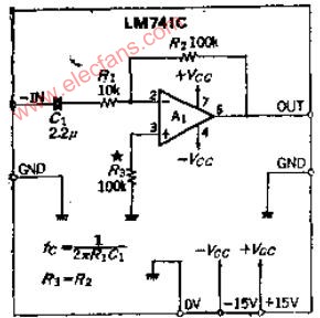
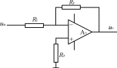
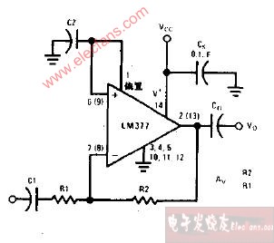
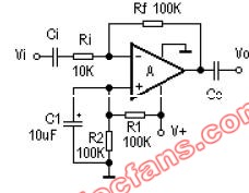
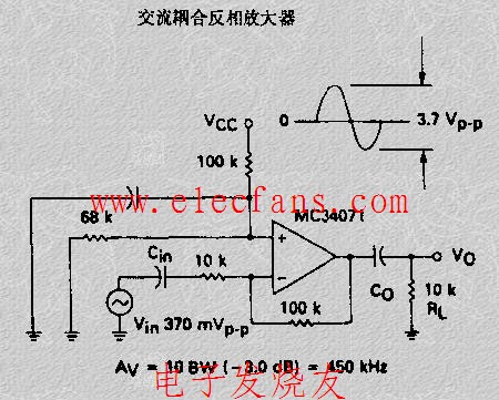
The basic operational amplifier circuit is shown in Figure 1. This circuit gives closed-loop gain of R2/R1 when this ratio is small compared with the amplifier open-loop gain and, as the name implies, is an inverting circuit. The input impedance is equal to R1. The closed-loop bandwidth is equal to the unity-gain frequency divided by one plus the closed-loop gain.
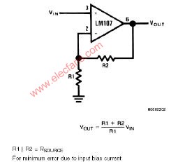
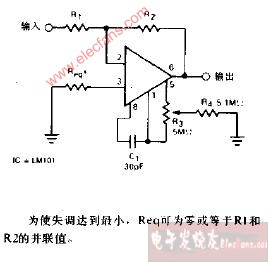
The only cautions to be observed are that R3 should be chosen to be equal to the parallel combination of R1 and R2 to minimize the offset voltage error due to bias current and that there will be an offset voltage at the amplifier output equal to closed-loop gain times the offset voltage at the amplifier input.
Offset voltage at the input of an operational amplifier is comprised of two components, these components are identified in specifying the amplifier as input offset voltage and input bias current. The input offset voltage is fixed for a particular amplifier, however the contribution due to input bias current is dependent on the circuit configuration used. For minimum offset voltage at the amplifier input without circuit adjustment the source resistance for both inputs should be equal. In this case the maximum offset voltage would be the algebraic sum of amplifier offset voltage and the voltage drop across the source resistance due to offset current. Amplifier offset voltage is the predominant error term for low source resistances and offset current causes the main error for high source resistances.
In high source resistance applications, offset voltage at the amplifier output may be adjusted by adjusting the value of R3 and using the variation in voltage drop across it as an input offset voltage trim.
Offset voltage at the amplifier output is not as important in AC coupled applications. Here the only consideration is that any offset voltage at the output reduces the peak to peak linear output swing of the amplifier.
The gain-frequency characteristic of the amplifier and its feedback network must be such that oscillation does not occur. To meet this condition, the phase shift through amplifier and feedback network must never exceed 180° for any frequency where the gain of the amplifier and its feedback network is greater than unity. In practical applications, the phase shift should not approach 180° since this is the situation of conditional stability. Obviously the most critical case occurs when the attenuation of the feedback network is zero. Amplifiers
which are not internally compensated may be used to achieve increased performance in circuits where feedback network attenuation is high. As an example, the LM101 may be operated at unity gain in the inverting amplifier circuit with a 15 pF compensating capacitor, since the feedback network has an attenuation of 6 dB, while it requires 30 pF in the non-inverting unity gain connection where the feedback network has zero attenuation. Since amplifier slew rate is dependent on compensation, the LM101 slew rate in the inverting unity gain connection will be twice that for the non-inverting connection and the inverting gain of ten connection will yield eleven times the slew rate of the non-inverting unity gain connection. The compensation trade-off for a particular connection is stability versus bandwidth, larger values of compensation capacitor yield greater stability and lower bandwidth and vice versa.
The preceding discussion of offset voltage, bias current and stability is applicable to most amplifier applications and will be referenced in later sections. A more complete treatment is contained in Reference 4.

基本的反相放大器电路示于图1。顾名思义,在R2/R1的数值远小于OP开环增益时,这个数值就是反相放大器的增益。输入阻抗就是R1的阻值,闭环增益带宽=单位增益带宽/(1+闭环增益)
在设计中需要注意的是:R3的阻值应该等于R1和R2的并联电阻,以减小输入偏置电流所带来的失调电压。输出失调电压=输入失调电压*闭环增益
OP输入端的失调电压有两个主要的来源,输入偏置电流(Input bias current)和输入失调电压(Input offset voltage)。对于一个给定的OP,输入失调电压就已经确定了,但是由输入失调电流所带来的失调电压与所采用的电路结构有关系,为了在不使用调整电路的情况下减小输入偏置电流所带来的失调电压,应该使得同、反相输入端对地的直流电阻相等,使得由于偏置电流在输入电阻上压降所带来的失调电压相互抵消。在对低内阻信号源的放大器中,OP的输入失调电压将成为失调电压误差的主要来源,而对于高内阻信号源的放大器,OP的输入偏置电流在信号源内阻上的压降将成为上述误差的主要来源。
在高输入阻抗的情况下,失调电压可以采用R3的阻值来调整,利用输入偏置电流在其上的压降来对输入失调电压作出补偿(既用这个的得到的压降来抵消输入失调电压)。
在交流耦合的时候,失调电压并不显得很重要,这时的主要问题是:失调电压减小了输出电压峰—峰值(P-P)的线性动态范围。
工作在闭环状态下的OP和其反馈网络的增益——频率特性,必须保证不会产生震荡。为了实现稳定,OP和反馈环路对任何频率的信号,在环路增益大于1时的环路相移角度绝对不能超过180°。在实践上,为了达到稳定条件,相移角度不应该接近180°。显然,最为临界的状态发生在反馈网络的衰减为0的时候(既跟随器状态)。没有做内部补偿的OP可以被用在深度反馈电路中以取得更好的频率特性。举一个例子:LM101在反相单位增益电路中,由于反馈网络6dB的衰减,仅需要15pF的补偿电容;但在同相单位增益电路中,由于反馈环路没有衰减,就需要30pF的补偿电容。由于OP的转换速度(SR)取决于补偿电容的大小, LM101的SR在反相单位增益电路里可以做到同相单位增益电路的2倍。反相电路在同等SR的条件下可以做到跟随器电路的110%。对于一个给定的OP放大器电路,在进行补偿时需要在稳定性和带宽之间进行进行权衡。加大补偿电容可以提高稳定性,但是牺牲了放大器的增益带宽,反之亦然。
 电子发烧友App










评论