全波整流器和平均值滤波器:The Full-Wave Rectifier and Averaging Filter
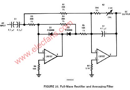
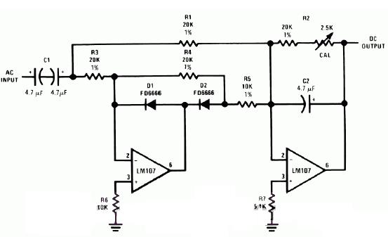
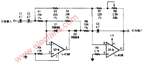
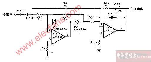
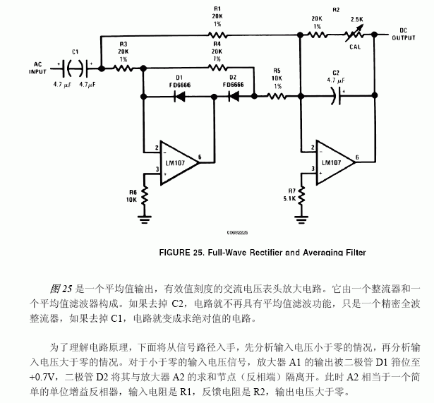
The circuit shown in Figure 25 is the heart of an average reading, rms calibrated AC voltmeter. As shown, it is a rectifier and averaging filter. Deletion of C2 removes the averaging function and provides a precision full-wave rectifier, and deletion of C1 provides an absolute value generator.
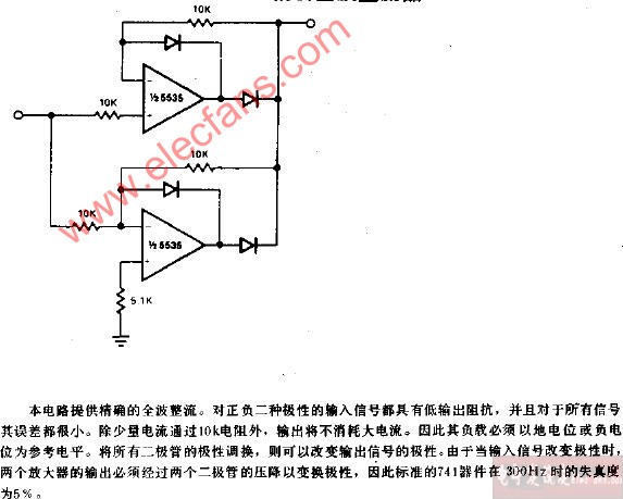
Circuit operation may be understood by following the signal path for negative and then for positive inputs. For negative signals, the output of amplifier A1 is clamped to +0.7V by D1 and disconnected from the summing point of A2 by D2. A2 then functions as a simple unity-gain inverter with input resistor, R1, and feedback resistor, R2, giving a positive going output.
For positive inputs, A1 operates as a normal amplifier connected to the A2 summing point through resistor, R5. Amplifier A1 then acts as a simple unity-gain inverter with input resistor, R3, and feedback resistor, R5. A1 gain accuracy is not affected by D2 since it is inside the feedback loop. Positive current enters the A2 summing point through resistor, R1, and negative current is drawn from the A2 summing point through resistor, R5. Since the voltages across R1 and R5 are equal and opposite, and R5 is one-half the value of R1, the net input current at the A2 summing point is equal to and opposite from the current through R1 and amplifier A2 operates as a summing inverter with unity gain, again giving a positive output.
The circuit becomes an averaging filter when C2 is connected across R2. Operation of A2 then is similar to the Simple Low Pass Filter previously described. The time constant R2C2 should be chosen to be much larger than the maximum period of the input voltage which is to be averaged.
Capacitor C1 may be deleted if the circuit is to be used as an absolute value generator. When this is done, the circuit output will be the positive absolute value of the input voltage.
The amplifiers chosen must be compensated for unity-gain operation and R6 and R7 must be chosen to minimize output errors due to input offset current.
图25是一个平均值输出,有效值刻度的交流电压表头放大电路。它由一个整流器和一个平均值滤波器构成。如果去掉C2,电路就不再具有平均值滤波功能,只是一个精密全波整流器,如果去掉C1,电路就变成求绝对值的电路。
为了理解电路原理,下面将从信号路径入手,先分析输入电压小于零的情况,再分析输入电压大于零的情况。对于小于零的输入电压信号,放大器A1的输出被二极管D1箝位至+0.7V,二极管D2将其与放大器A2的求和节点(反相端)隔离开。此时A2相当于一个简单的单位增益反相器,输入电阻是R1,反馈电阻是R2,输出电压大于零。
输入大于零时,A1起放大作用,输出经电阻R5连到A2的求和节点。放大器A1接成一个简单的单位增益反相器,输入电阻是R3,反馈电阻是R5(此处反馈电阻应该为R4,疑原文笔误——译者)。由于D2位于反馈环路之内,所以它不会影响A1的增益精度(译者认为有误,见注释1)。正向电流经R1流入A2的求和节点,反向电流经电阻R5流出A2的求和节点。由于R1和R5上的电压大小相等方向相反,而且R5的阻值是R1的1/2,所以A2的求和节点处的电流与R1上的电流大小相等流向相反,(译者认为有误,见注释2)此时A2构成一个单位增益反相加法器,输出仍然为正值。
在R2上跨接电容C2,构成了一个平均值滤波器。此时A2的作用与前文所述的“简单低通滤波器”相似。R2C2的时间常数必须仔细选取,使其远远大于输入电压的最长平均周期。
如果去掉电容C1,本电路就会变成一个计算绝对值的电路,即电路输出将等于输入电压的绝对值。
 电子发烧友App









评论