In-Circuit Programming for the MAX16046–MAX16049 EEPROM-Programmable System Managers
Abstract: The MAX16046,MAX16048,MAX16047,MAX16049 system managers can be programmed after being soldered to the application circuit board. This means that only unprogrammed devices need to be stocked, and that the latest version of the configuration information can be written to the device during manufacturing test. A few simple measures ensure that the application circuit allows the programming hardware to share the I²C or JTAG bus line and provides power for the device during programming. The programming algorithm is provided for both the I²C bus and the JTAG bus.
The MAX16046–MAX16049 EEPROM-programmable system managers are power-supply sequencers, monitors, and marginers that can control up to 12 power supplies. Power supplies are monitored by three digital comparators, margined by programmable DAC outputs, and sequenced with a programmable state machine.
These system managers include an SMBus™-compatible I²C interface and a JTAG interface, both of which can access all device registers and program the internal configuration EEPROM. The MAX16046–MAX16049 are in-circuit programmable, as long as a few simple guidelines are followed.
Providing Power
The MAX16046–MAX16049 have a supply voltage range of 3V to 14V. Typical applications connect VCC to a 12V intermediate bus voltage or a 3.3V auxiliary supply.
It is possible to program the MAX16046–MAX16049 with a partially powered board. For example, the 3.3V auxiliary voltage could be applied without any other supplies, or the 12V intermediate bus voltage could be applied; all downstream power supplies should be off since the system manager is not programmed at that point. Another option is to use a commonly available dual diode to allow power to be supplied from a programming connector. Due to the voltage drop caused by the diode, this approach works best when the MAX16046–MAX16049 is powered from a 12V bus.
If diode OR-ing is not used and the MAX16046–MAX16049 are to be programmed with power applied to the board, careful attention must be paid to the state of the sequencing outputs to prevent any downstream power supplies from prematurely turning on.
When unprogrammed, the MAX16046–MAX16049 have high-impedance outputs. Power supplies with active-high enable inputs should have pulldown resistors, and power supplies with active-low enable inputs should have pullup resistors. The sequencing outputs can be configured as either push-pull or open-drain. Because the open-drain configuration requires an external pullup resistor, it should be used with active-low enable inputs only.
It is not advisable to connect the MAX16046–MAX16049 in a JTAG chain, as power may not be applied to upstream devices in the chain, effectively cutting off access to the MAX16046–MAX16049. Rather, a JTAG multiplexer or a dedicated JTAG port is preferred.
Sharing the Bus
A potential problem occurs when a device, other than the µP, needs to communicate with the MAX16046–MAX16049 during normal operation. One example is when a system supervisory µP needs to access the ADC readings of the MAX16046. When the board is unpowered or partially powered and the MAX16046 is being programmed, other devices connected to the I²C or JTAG bus could interfere. The easiest solution is to program the MAX16046 through the JTAG interface and connect the supervisory µP to the I²C interface. If the µP supports true open-drain I²C bus I/O (that is, pins that lack the ESD diode to VCC) and the pullup resistors are large enough, it can be possible to share the I²C bus for both programming and normal operation. If the µP's I²C bus lines are not open-drain, the ESD diodes will clamp the bus lines and interfere with programming.
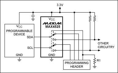
If the system µP does not have true open-drain I²C bus lines, a circuit like the one in Figure 1 can be used to automatically switch between the µP and the programming I²C bus.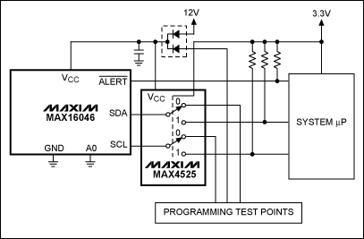
Figure 1. The MAX16046 shares its I²C bus through the MAX4525 multiplexer/switch.
The MAX4525 multiplexer in Figure 1 switches between the I²C connected to the system µP and the I²C connected to the programming test points. The switch is controlled by the VCC of the system µP. If VCC is not applied, but 12V is, the switch connects I²C to the programming test points. Once VCC is applied, the switch connects the I²C to the system µP.
Application Circuit Examples
The following figures show three different application circuits designed for in-circuit programming.
Powered from a 12V Intermediate Bus and Programmed through the I²C Bus
The Figure 2 circuit powers the MAX16046 from the 12V intermediate bus, which is monitored by the analog enable line, EN. When the 12V bus rises above the threshold set by the resistive divider on EN, the MAX16046 attempts sequencing if it has been programmed. An unprogrammed MAX16046 does not do anything, and the sequencing outputs remain at a high impedance level.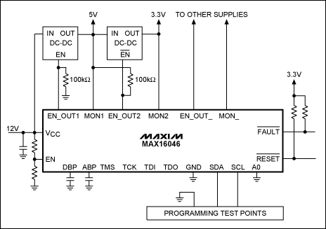
Figure 2. The MAX16046 is powered from the 12V intermediate bus and programmed through the I²C interface.
One power supply uses an active-high, push-pull enable signal, and the other uses an active-low, open-drain enable signal. Appropriate pullup and pulldown resistors prevent these power supplies from turning on while the unprogrammed outputs are at a high impedance level.
It is important to note that push-pull outputs cannot be pulled up above VDBP, and that open-drain outputs cannot be pulled up above 6V. The I²C connections are brought out to programming test points; appropriate pullup resistors must be provided by the programming hardware. The circuit is simple because no other device on the circuit board needs to connect to the I²C bus.
Powered from a 3.3V Auxiliary Supply and Programmed through a JTAG Multiplexer
In Figure 3, the MAX16046 derives power from a 3.3V auxiliary supply. The JTAG connections are shared with other devices using a DS29600 JTAG multiplexer that is also powered from the 3.3V auxiliary supply. Programming can be accomplished by providing 3.3V without needing to power up the 12V intermediate bus.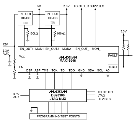
Figure 3. The MAX16046 is powered from a 3.3V auxiliary supply and programmed through the DS26900 JTAG multiplexer.
Powered from a 12V Intermediate Bus and Programmed through JTAG
Figure 4 shows the MAX16046 powered with a diode-OR'ed connection to the 12V intermediate bus so that power may safely be applied without powering on any downstream power supplies. The JTAG and power connections are brought out to programming test points.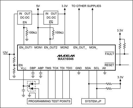
Figure 4. The MAX16046 is powered from a 12V intermediate bus and programmed through JTAG.
Programming Algorithm
The MAX16046–MAX16049 have built-in EEPROM that stores the device configuration parameters. When power is applied, the contents of the EEPROM are transferred to the RAM registers. Both RAM and EEPROM are accessible from the JTAG and I²C interfaces. To correctly program the MAX16046–MAX16049, the desired parameters must be programmed to the EEPROM—see the memory map in Table 1.
Table 1. MAX16046 Memory Map 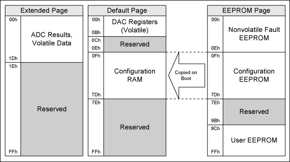
Configuration Files
The MAX16046 evaluation kit (EV kit) software provides two types of configuration files. One is a human-readable XML file produced by selecting File Save Configuration As. This file can be used for I²C programming. The second is produced by selecting File Save as .SVF. This file is in the serial vector format (SVF) used by third-party JTAG tools and in-circuit PCB testers for JTAG programming.
The XML file may be viewed in a color-coded hierarchical format in many web browsers. The XML file generated by the EV kit software is divided into several sections and contains setup tab information as well as register data. There are two sections of interest: the Config_Register section, which contains configuration values that can be loaded into EEPROM, and the User_Register section, which contains values to load into the user EEPROM.
Within each section, a Register tag specifies the value to be loaded into a particular address. The format of the register tag is as follows:
All values are decimal. These addresses correspond to both RAM registers and EEPROM addresses. Be aware that RAM registers 0 to 14 are DAC registers, but EEPROM at address 0 to address 14 is saved fault data. EEPROM programming routines should start at address 15.
Details on the XML file format can be found at the XML Developer Center.
The SVF file format is described in more detail in the Serial Vector Format Specification (PDF, 85.2KB).
I²C Programming Procedure
To program the MAX16046–MAX16049's EEPROM-configuration memory, it is necessary to first make sure that the configuration-lock bit in register r5Dh[0] is zero. If it is not zero, write a '1' to that bit to clear it. To write to the EEPROM, send the appropriate command to enter the EEPROM page, load the starting address, and send a series of block-write commands. See the MAX16046/MAX16048 or MAX16047/MAX16049 data sheet for details on their respective I²C protocols.
Pseudocode for a typical EEPROM programming process is as follows:
SendByte(5Dh)                 // Check lock bit
If ReadByte() & 2 == 2 Then
WriteByte(5Dh, 02h)         // Clear lock bit if needed
SendByte(9Ah)                 // Access EEPROM page
Loop Address from 0Fh to 7Dh
  SendByte(Address)           // Load address
  WriteBlock(Data, 10h)       // Write a block of 16 bytes
  Wait(16 * 11 milliseconds)  // Wait for programming
SendByte(Address)
ReadBlock(DataRead, 10h)    // Read back data block
If DataRead != Data Then
  RepeatCount = RepeatCount + 1
  If RepeatCount == 3 Then
    Fail
Else
  RepeatCount = 0
  Address = Address + 10h   // Advance to next block
SendByte(9Bh)                 // Return to default page
Success
To write to the user EEPROM, the same process may be used, but with an address range of 9Ch to FFh instead of 0Fh to 7Dh.
JTAG Programming Procedure
Use standard third-party JTAG tools, the MAX16046 BSDL file, and an SVF data file generated by the EV kit software to program the MAX16046–MAX16049 with either a JTAG programming cable or an in-circuit PCB tester. The BSDL file can be downloaded from the Maxim website.
 电子发烧友App




评论