摘要:某些应用程序要求输入偏移电压(V 操作系统 )的电流检测放大器进行校正 , 以提高测量精度。 This is not a straightforward task because of interactions between the output voltage low (V OL ) and the input V OS . 这不是因为输出电压之间的低(五职等 )和输入的 V OS相互作用简单的任务。 This application note outlines a simple method to artificially "skew" the input V OS of unidirectional current-sense amplifiers. 本应用说明概述了一个简单的方法 , 人为地“倾斜”的输入电压V OS的单向电流检测放大器。 The method allows measurement of total-input V OS without the normal limitations from V OL , and improves the overall accuracy of current measurements. 该方法可以测量总投入的 V OS从V 职等不正常的限制,提高了整体的电流测量精度。 The MAX4080 current-sense amplifier serves as the example of the technique. 在MAX4080电流检测放大器作为该技术的例子。
A similar version of this article was published on March 23, 2009 on the Planet Analog website.这个类似文章发表在2009年3月23日在地球模拟网站。
Introduction导言
Current-sense amplifiers are sophisticated ICs, popular in electronic equipment that monitors load currents in real time.电流检测放大器是复杂的集成电路,电子设备,实时监测,负载电流受欢迎。 System controllers use this load information to implement power-management algorithms that modify the load-current characteristic itself, and to implement flexible overcurrent protection schemes.系统控制器使用此负载信息来实现电源管理算法,修改负载电流特性本身,并实施灵活的过电流保护计划。
Current-sense amplifiers magnify a small differential voltage while rejecting the input common-mode voltage.电流检测放大器放大小差分电压,同时拒绝输入共模电压。 In this role they operate like traditional op amp-based differential amplifiers.在这个职位上工作一样,他们的传统运算放大器的差分放大器。 There is, however, an important difference between these two amplifier architectures.然而,这两个之间的放大器架构的重要区别。 The input common-mode voltage for current-sense amplifiers is allowed to exceed the power-supply (V CC ) voltage.输入共模电流检测放大器电压可以超过电源,电源(V CC)的电压。 When, for example, the MAX4080 current-sense amplifier is powered from V CC = 5V, it can still withstand an input common-mode voltage of 76V.时,例如,MAX4080电流检测放大器是由V CC = 5V供电电源,它仍然可以承受的76V输入共模电压。 By using unique amplifier architectures, current-sense amplifiers are not hampered by the common-mode rejection limitations (CMRR) that arise from mismatched resistors.通过使用独特的放大器架构,电流检测放大器不是由共模抑制限制(共模抑制比),从匹配电阻产生的阻碍。 The MAX4080, for example, has 100dB (min) DC CMRR.在MAX4080,例如,为100dB(最小)直流的CMRR。 In contrast, the performance of traditional op amp-based differential amplifiers is negatively impacted by CMRR, and their effective input V OS is magnified through the signal chain.相比之下,传统运算放大器的性能是基于差分放大器的CMRR负面影响,其有效投入的 V OS是通过信号链放大。 
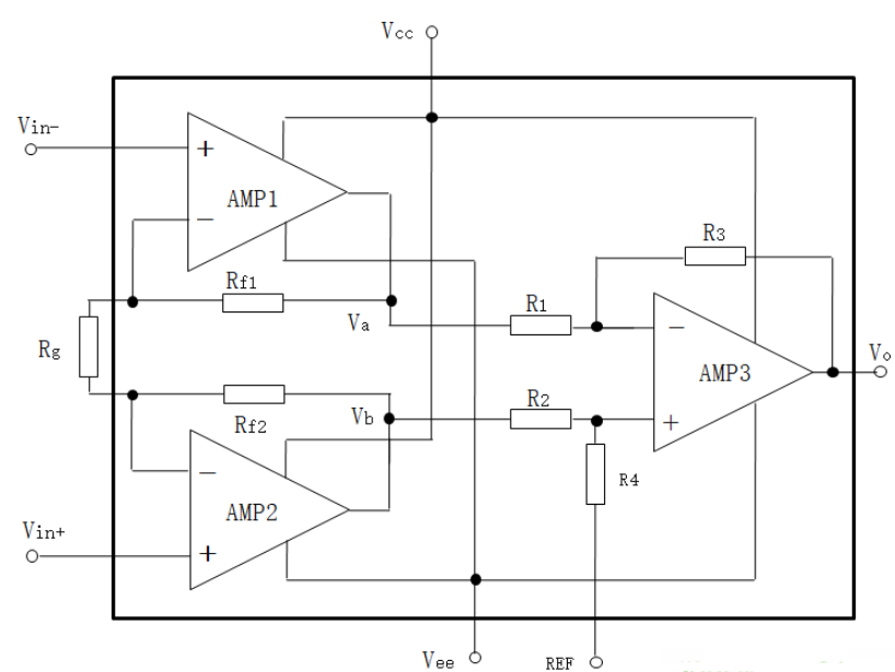
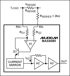
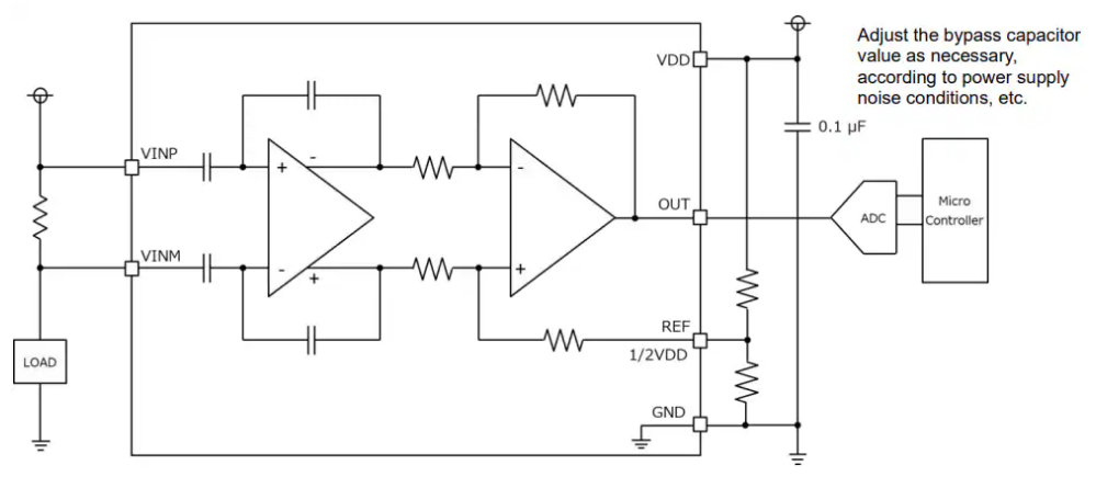
Figure 1. 图1。 The MAX4080 is a precision unidirectional current-sense amplifier. 在MAX4080是精密单向电流检测放大器。
Using Calibration to Improve Precision使用校准精度提高
The MAX4080 has a precision ±0.6mV (max) input offset voltage (V OS ) at 25°C, and ±1.2mV (max) V OS over the -40°C to +125°C temperature range.在MAX4080具有精度± 0.6mV(最大值)在25 ° C输入失调电压(V OS),然后在-40℃± 1.2mV(最大值) 的 V OS至+125 ° C温度范围。 Some applications, however, need to further calibrate input V OS to enhance precision of the final current measurement.一些应用程序,但是,需要进一步校准输入的 V OS,以加强最后电流测量精度。 To do this calibration, V OS is typically measured during production and stored in firmware.要做到这一点校准,第五操作系统通常是在生产过程中测量和固件中。 This V OS is then adjusted digitally in real time when the equipment is in the field and in use.这一V 操作系统 ,然后调整实时数字设备时,在外地和正在使用中。
A preferred method of calibration, intended for the convenience of manufacturing, would measure the V OS when there is zero load current (zero input differential voltage).阿标定的首选方法,对拟生产的方便,将测量的 V OS为零时,负载电流(零输入差分电压)。 In this approach one could measure the output V OS and subtract this voltage from all future measurements.在这种方式人们可以测量输出V OS和减去所有未来的测量这个电压。 Unfortunately, this method has a drawback.不幸的是,这种方法有一个缺点。 The V OL (output voltage low) and input V OS specifications interact, causing the output voltage not to reflect the input V OS accurately. 其他职等的V(输出电压低)和输入的 V OS规格的互动,导致输出电压没有体现出输入的 V OS准确。 This interaction is, in fact, characteristic of all single-supply amplifiers.这种互动,实际上,所有的特征单电源放大器。
Consider the example of the MAX4080T with a gain of 20, and hypothetical zero input V OS .考虑MAX4080T为20增益的例子,假设零投入的 V OS。 One would then expect to measure a true zero at the amplifier's output.由此便期待着在测量放大器的输出真正的零。 However, even at zero input differential voltage, the amplifier is not guaranteed to output a voltage below 15mV (with 10µA sink current).然而,即使在零输入差分电压,放大器不能保证输出电压低于15mV(带10μA的吸收电流)。 In fact, if the output voltage measurements were used directly for V OS calibration, the amplifier would appear to have a 0.75mV input V OS (15mV/20 = 0.75).事实上,如果输出电压测量被用于校准的 V OS直接,放大器似乎有0.75mV输入的 V OS(15mV/20 = 0.75)。
Similarly, if a MAX4080T did have V OL = 0, then a positive input V OS will produce a positive output V OS as expected.同样,如果MAX4080T确实有V 职等 = 0,则积极投入的 V OS将产生积极输出V 操作系统预期。 However, a negative input V OS will not be "reflected" in the output voltage measurement, since the amplifier cannot really output a voltage below ground.然而,消极的输入电压V OS将不会是“反映在输出电压的测量”,因为不能真正放大器输出电压低于地面。 Thus to summarize, one cannot "directly" use an output voltage measurement with zero input differential voltage to calibrate the input V OS .因此,要总结,不能“直接”使用零输入差分电压的输出电压测量校准输入的 V OS。
There are two methods typically used to calibrate V OS during production:通常有用于校准在生产过程中的 V OS两种方法:
- A bidirectional current-sense amplifier like the MAX4081 is used with a reference voltage of about 1.5V.阿双向电流,如检测放大器MAX4081使用约1.5V的参考电压。 This effectively translates the output voltage measurements by 1.5V, so a zero input differential voltage will output 1.5V ±V OS -induced errors.这有效地转换了1.5V的输出电压测量,所以零输入差分电压输出1.5V的± 的 V OS引起的误差。 Since this 1.5V voltage is well above the amplifier's V OL , it does not affect error analysis.由于这1.5V的电压远高于放大器的V 职等 ,它不会影响误差分析。 V OS errors can thus be calculated by measuring the difference between the output voltage and the ideal 1.5V input reference voltage. 的 V OS错误,因此可以通过测量计算之间的输出电压和1.5V的理想的输入参考电压差异。 There is a drawback to this method: reduced dynamic range.目前对这一方法的缺点:降低动态范围。 The 0 to 5V input dynamic range of the device's ADC is now reduced 30% to 1.5V to 5V).在0至5V的输入动态范围的器件的ADC现在降低了30%至1.5V至5V)。 Additionally, the method requires a more expensive bidirectional current-sense amplifier to be used for unidirectional measurements.此外,该方法需要更昂贵的双向电流检测放大器,用于单向测量。 Finally, generating a low-drift 1.5V reference voltage or spending a second channel to measure this 1.5V reference voltage is not attractive.最后,产生一个低漂移1.5V的参考电压或支出第二个通道来衡量这一1.5V的参考电压是没有吸引力。
- A two-point measurement method is employed in which two known values of a differential input voltage (load currents) are applied to the current-sense amplifier.阿二点的测量方法是采用在两个已知的差分输入电压(负载电流)值应用到电流检测放大器。 First, straight-line approximation is applied to the output voltage measurements to calculate the input V OS by extrapolating to a zero-sense voltage.首先,直线近似适用于输出电压测量计算推算为一个零检测电压输入的 V OS。 Secondly, that voltage measurement is then used for calibration.其次,电压测量然后用于校准。 This method has its drawback: it uses two "known" exact values of currents during production, which is inconvenient and increases test time.这种方法有它的缺点:它使用了两个“之称的”生产过程中的电流的精确值,这是不便并增加测试时间。 Finally, accurate measurements close to a zero input differential voltage are still not achieved because V OL limitations will cause errors at small sense voltages.最后,精确的测量接近零输入差分电压仍然没有实现因为V 职等限制,将导致在检测电压误差小。
Using Input Resistors to Introduce Input V OS使用输入电阻将推出输入的 V OS
This application note presents a third method for measuring the input V OS of a current-sense amplifier.本应用笔记介绍了测量输入的 V OS的电流检测放大器三分之一的方法。 Once again, the MAX4080 serves as the example.再次MAX4080作为例子。 This approach applies a zero input differential voltage and overcomes the interactions between V OL and V OS —making it easy to use on the production line.这种方法适用于一零输入差分电压和克服这是由V和V 操作系统职等的相互作用,从而易于使用的生产线。
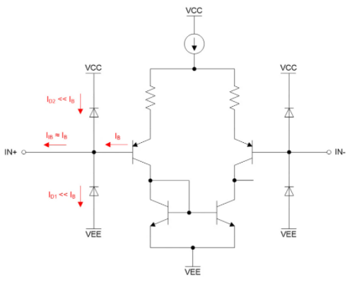
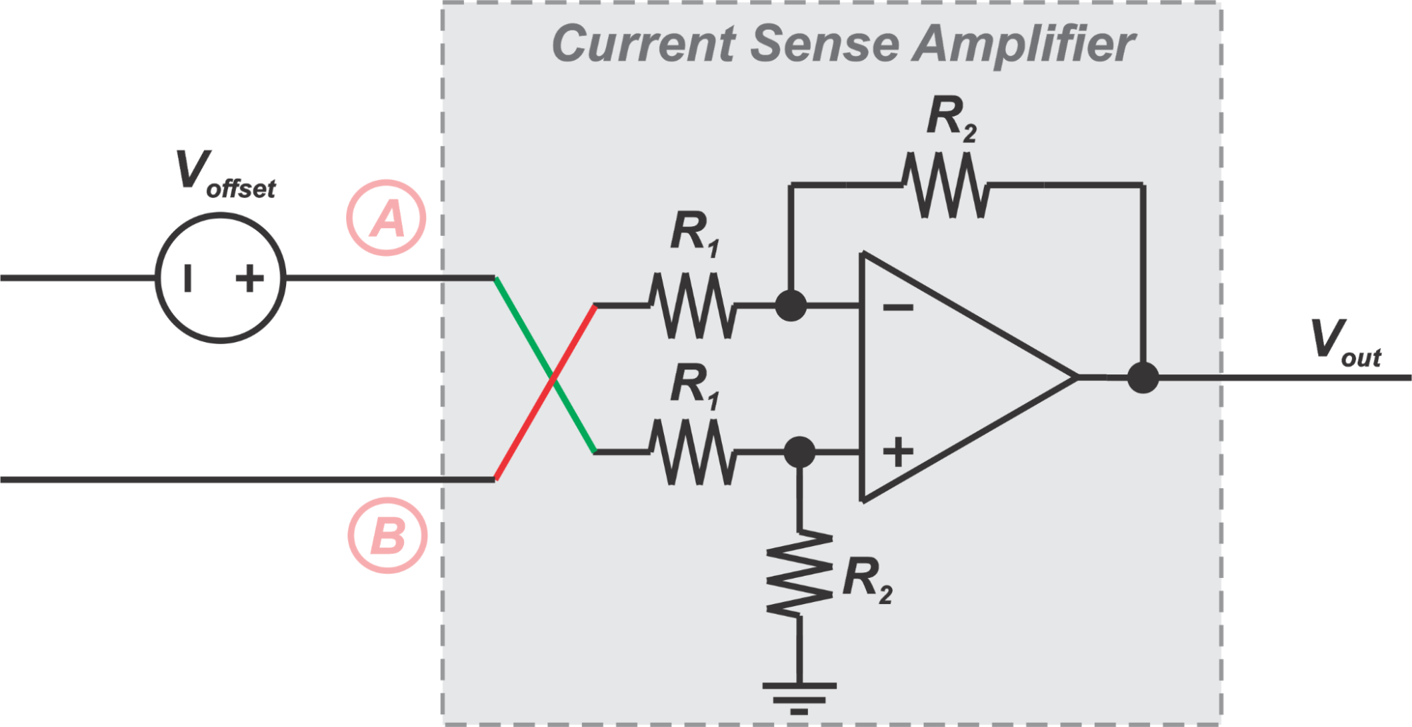
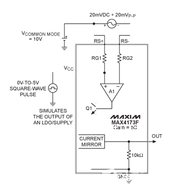
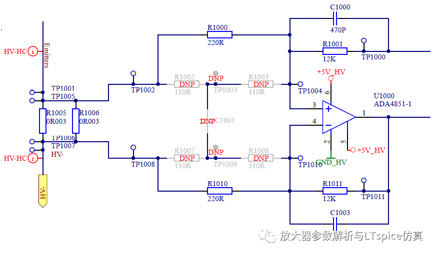
All current-sense amplifiers have input bias currents.所有的电流检测放大器的输入偏置电流。 Therefore the use of input resistors (for input filtering, as an example) should be carefully studied since the resistors can introduce unplanned gain and offset errors.因此,使用的输入电阻(用于输入过滤,为例)应小心,因为电阻可以引进计划外增益和失调误差研究。 These issues are detailed in application note 3888, " Performance of Current-sense Amplifiers with Input Sense Resistors ."这些问题的详细应用笔记3888“ 的电流检测电阻与输入感觉放大器的性能 。” The method presented here uses similar techniques, but in this case, the input resistors are intentionally mismatched.这里介绍的方法使用类似的技术,但在这种情况下,输入电阻是有意不匹配。 In this manner an intentional output V OS is introduced.在这种有意输出V OS是提出的方式。 The MAX4080 has a temperature-compensated bias current of 5µA (typ) and 12µA (max) over process variation.在MAX4080有一个温度补偿偏置电流降至5μA(典型值)和12μA的(最大值超过过程变化)。 Using a 2kΩ resistor in series with RS- ( Figure 2 ) thus produces a typical input V OS of 10mV and 24mV, respectively, over process variation.使用与RS系列2kΩ电阻( 图2),从而产生对过程变化的典型输入有10mV和24mV,分别的 V OS。 This additional input V OS then causes an output offset of 200mV (typ) and 480mV (max), which is adequate to override any V OL and V OS limitations in the basic MAX4080.这种额外的输入电压V 操作系统然后200mV的原因(典型值)抵销了产量和480mV(最大),这足以覆盖的基本MAX4080任意V 职等和V 操作系统的限制。 Error in this input-resistor-induced V OS will have a temperature dependence based both on the drift characteristics of the input resistor (usually 100ppm) and on the bias current (negligible).在此输入错误电阻引起的 V OS将有一个温度特性基础上,输入电阻(通常为100ppm)的漂移特性都和偏置电流(忽略不计)。 
Figure 2. 图2。 The MAX4080 configured to use an external 2kΩ resistor in series with RS-. 在MAX4080配置为使用外部2kΩ的与RS系列电阻。
The resistor drift characteristic of +100ppm causes a +1% change in the resistance value over a 100°C change (ie, +20Ω).在100分之电阻漂移特性导致超过100℃的变化在1%的电阻值的变化(即20Ω)。 Additional input V OS drift from the input resistor is then typically about +0.1mV, and +0.24mV max across the process variation of bias current.额外投入的 V OS漂移的输入电阻,然后通常约为0.1 mV时,和0.24整个过程中的偏见压变化最大电流。 This drift is still only 20% of the ±0.6mV bidirectional error in input V OS that one would usually expect from process variation if no calibration were used.漂移仍只有20%的± 0.6mV在双向输入错误的 V OS,一个通常会期望从工艺变化,如果没有被用来校准。
Decreasing the size of the input series resistor further reduces this drift error.减少了输入串联电阻的大小,进一步降低此漂移误差。 To account for the 15mV V OL and the ±1.2mV input V OS over temperature, the additional input V OS would need to be a minimum of 1.2mV + 15mV/20 = 1.95mV = 2mV, approximately.以考虑到15mV V 职等及以上温度的± 1.2mV输入的 V OS,增加投入的 V OS将需要最低限度的1.2mV + 15mV/20 = 1.95mV = 2mV,大约。 Table 1 shows the test results over temperature.表1显示温度的测试结果。 Here, the MAX4080 has negligible drift in V OS , and so all measured drift in V OS is due to the use of input resistor and its ppm drift.在这里,MAX4080在微不足道的 V OS漂移,因此所有测量漂移在V OS是由于输入电阻和漂移的百万分之使用。
Table 1. 表1。 Results of Temperature Tests With and Without Input Resistors 温度测试结果有和没有输入电阻
| V OS 的 V OS | -40°C -40℃ | +25°C +25℃ | +85°C +85℃ | +125°C +125℃ |
| No Input Resistors没有输入电阻 | -0.015mV - 0.015mV | 0mV 0mV | -0.005mV - 0.005mV | -0.01mV - 0.01mV |
| 2kΩ in Series with RS-在系列2kΩ的带有RS - | 9.69mV 9.69mV | 9.73mV 9.73mV | 9.76mV 9.76mV | 9.80mV 9.80mV |
Conclusion结论
This application note presents a method that introduces known input V OS by suitably sizing input resistors for current-sense amplifiers like the MAX4080.本应用笔记介绍了,介绍已知的适当大小的电流,如MAX4080检测放大器输入电阻输入的 V OS方法。 Equipment manufacturers can thus use this methodology for production-line calibration of V OS with zero input current to enhance the accuracy of real-time measurements.因此,设备制造商可以使用输入电流为零,以提高实时测量精度的方法,这种生产线的V 操作系统校准。
 电子发烧友App












评论