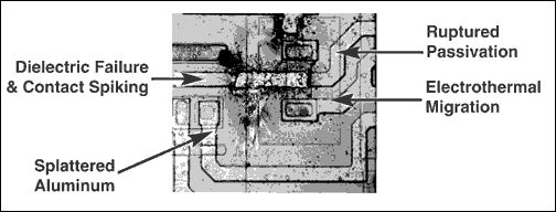
Electrostatic discharge (ESD) can threaten an electronic system when someone replaces a cable or even touches an I/O port. Discharges that accompany these routine events can disable the port by destroying one or more of its interface ICs (Figure 1). Such failures can also be costly—they raise the cost of warranty repairs while diminishing the product's perceived quality.

Figure 1. ICs with inadequate ESD protection are subject to catastrophic failure—including ruptured passivation, electrothermal migration, splattered aluminum, contact spiking, and dielectric failure.
ESD has another way of causing trouble. Manufacturers may soon be barred from selling to the European community unless their equipment meets minimum levels of ESD performance. These two factors, coupled with the increasing amount of electrical communication between computers and computer-related equipment, lend emphasis to the need for engineers to understand ESD.
A proper understanding of ESD requires an awareness not only of the voltage levels involved, but also of the voltage and current waveforms, IC-protection structures, test methods, and application circuits. These matters are discussed in the following sections.
ESD Generation
Electrostatic charge appears when two dissimilar materials come together, transfer charge, and move apart, producing a voltage between them. Walking on a rug with leather soles, for example, can generate voltages as high as 25kV. The level of electrostatic voltage induced depends on the relative charge affinity between rug and shoe leather, the humidity, and other factors.The triboelectric series (Table 1) describes this charge affinity between various materials. Charge transfer occurs when any two items on the list are brought into contact. Materials higher in the series acquire positive charge, and those lower in the series acquire negative charge.1 The net charge and resulting electrostatic voltage is greater for items farther apart on the list.
Table 1. Triboelectric Series

ESD Test Methods
Two methods are commonly used for testing the ESD susceptibility of integrated circuits. The oldest, MIL-STD-883 Method 3015.7, was developed as an aid in understanding the precautions necessary for packaging and handling ICs. This method tests each package pin against other groups of pins, and classifies the device according to the lowest voltage for which failure occurs.The applied signal in this test is a current waveform derived from a circuit called the human body model (Figure 2), which simulates the capacitance and source impedance typical of a human body. (Circuit layout is critical, because the actual waveform delivered at the IC depends also on parasitic inductance and capacitance associated with the test connections and pc board.) The resulting current waveform represents the ESD that occurs when a person touches an object, such as an IC.

Figure 2. Substituting different component values as shown yields discharge circuits known as the human body model, the machine model, and the IEC 1000-4-2 model (human holding a metallic object).
The other method, which differs from the above only in the values for R and C, was developed by the Electronic Industries Association of Japan (EIAJ). Called IC-121 and based on a circuit called the machine model (Figure 2), it applies a current waveform similar to that produced when an IC makes contact with its handling machinery. By mimicking the ESD events caused by charges that accumulate on moving parts, the waveform simulates static discharges seen during machine assembly.
The two methods are complementary, so you shouldn't choose one over the other. Because ESD can affect ICs during manufacturing, during pc board assembly, and after the end product is put into service, a test based on the human body model and the machine model together provides adequate assurance regarding the IC's tolerance for the rigors of manufacturing and insertion.
Some ICs, whose pins are exposed to the outside world through connectors, can encounter ESD even when mounted on a pc board within an enclosure. ESD exposure is less likely for the other pins, which are connected to circuitry on the board. For this class of IC, a test method such as Method 3015.7 (which tests pin combinations) does not provide an adequate representation of ESD susceptibility for the input/output (I/O) pins.
Both offer ratings according to the lowest-voltage failure on any pin-an approach that may not do justice to the higher levels of internal ESD protection required by the I/O pins (and provided by some manufacturers). A device might have I/O pins that withstand ±15kV, for example, and non-I/O pins that fail at ±2kV. With the above methods, the device's ESD rating would be less than ±2kV. Fortunately, however, better test methods are now available for rating the I/O pins.
New ESD Tests for I/O Ports
An I/O port allows communication with other pieces of equipment. I/O ports for ICs comprise logical groups of pins that give access to equipment external to the system that contains the IC. These pins are subject to static discharge and other abuse as operators connect and disconnect cables from the system. For the I/O pins of an RS-232 or RS-485 interface IC, an ideal test method for ESD susceptibility should:- Test the I/O pins only in ways that simulate exposure to ESD events in actual equipment.
- Apply test waveforms that model electrostatic discharges produced by the human body. Different circuit models specify different values of amplitude, rise/fall time, and transferred power.
- Test the IC with and without power applied.
- Define IC failures to include latchup (a momentary loss of operation), as well as catastrophic or parametric failure. Latchup is considered a failure mechanism because if left undetected, it can lead to reliability problems and system malfunctions.

Figure 3. This ESD waveform's parameters (rise time, peak current, ringing, and decay time) are specified in MIL-STD-883 method 3015.7.
Like the original Method 3015.7, the modified method defines only an ESD waveform and the criteria for failure: after exposure to the waveform, a failed IC must either exhibit latchup or fail one or more data sheet specifications. The modified method stipulates no particular operating mode for the IC during test, but Maxim recommends that all possible modes be exercised: power on/off, transmitter outputs high/low, standby/normal operation, etc.
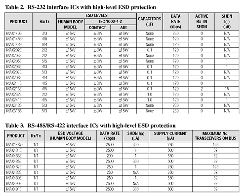
Similarly, the modified method 3015.7 does not compel products to withstand particular levels of ESD; it only defines classes of protection. New transceivers from Maxim, however, generally provide protection levels to ±15kV (Tables 2 and 3). This level allows some users to eliminate costly TransZorbs™; and other external protection circuitry.
IEC 1000-4-2 Model
The second, more stringent method for testing ICs that include I/O pins is IEC 1000-4-2. This equipment-level test was developed by the International Electrotechnical Commission. Originally intended as an acceptance condition for equipment to be sold in Europe, it is rapidly gaining acceptance as a standard ESD criterion in the United States and Japan as well. Though not originally intended as an IC specification, it now does extra duty as an ESD test for ICs. Like the modification to 3015.7, it tests only the I/O pins.The model for IEC 1000-4-2 is again the circuit of Figure 2, but with different component values. The resistance R2 (330Ω) represents a human holding a screwdriver or other metallic object, and C1 (150pF) represents another estimate of human-body capacitance. This circuit produces a current waveform (Figure 4) with a rise time steeper than that produced by Method 3015.7.

Figure 4. Parameters for this ESD waveform (rise time, peak current, amplitude at 30ns, and amplitude at 60ns) are specified by IEC 1000-4-2.
IEC 1000-4-2 specifies ESD testing both by contact discharge and by air discharge. ESD events caused by actual contact are more repeatable but less realistic, and air discharge is more realistic but subject to wide differences in waveform shape—according to variations in temperature, humidity, barometric pressure, distance between IC and electrode, and rate of approach to the IC pin. (This change of shape can have a significant effect on the measured level of tolerance for ESD.)
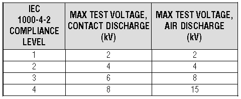
IEC 1000-4-2 defines four levels of compliance (Table 4) according to the lowest maximum voltage withstood by the I/O pins. The table defines these levels both for contact discharge and for air discharge.
Table 4. IEC 1000-4-2 Compliance Levels
Contact or Air Discharge?
Testing ICs for ESD ruggedness per IEC 1000-4-2 requires the use of an ESD "gun," which allows testing with either contact discharge or air discharge. Contact discharge requires physical contact between the gun and the I/O pin before test voltage is applied by a switch internal to the gun. Air discharge requires the gun to be charged with test voltage before it approaches the I/O pin (from the perpendicular, and as quickly as possible). The second technique produces a spark at some critical distance from the test unit.ESD produced by air discharge resembles actual ESD events. But, like actual ESD, the air-discharge variety is not readily duplicated. It depends on many variables that are not easily controlled. Thus, attesting to the general importance of repeatability in testing, IEC 1000-4-2 recommends contact discharge, and the modified 3015.7 method requires contact discharge only. In either case, the test procedure calls for at least 10 discharges at each test level.
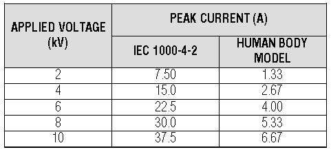
The main difference between the two ESD standards just discussed—the modified 3015.7 method and the air- or contact-discharge version of IEC 1000-4-2—is in the peak currents they produce in the device under test. Different component values can cause these peak currents to differ by a factor greater than five (Table 5). Because peak currents produce the unwanted power that an IC must dissipate, IEC 1000-4-2 is usually the more demanding test method for ESD.
Table 5. ESD Current vs. Model and Applied Voltage
High current can damage an IC in various ways:
- Excessive local heating
- Melted silicon
- Spiked junctions, caused by a short that dissolves aluminum in the silicon (Figure 5)
- Damaged metal lines
- Gate-oxide failure due to excessive voltage
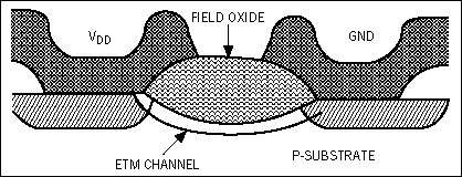
- Transistor damage due to electrothermal migration (Figure 6)

Figure 5. High-ESD current in an IC can "spike" a junction by partially dissolving the aluminum contact in silicon, causing a permanent short to the layer below.

Figure 6. Electrothermal migration (ETM) in an IC can set the stage for damage in the presence of an ESD event. The resulting high current and high voltage can cause a short circuit or low-impedance path between the terminals of a transistor.
Protection Methods
To protect against ESD, a designer can either add the protection externally or choose ICs with high levels of protection built in. Protection circuitry includes metal-oxide varistors and silicon avalanche suppressors such as the TransZorb. These devices are effective but expensive (silicon avalanche protectors cost as much as $0.30 per line). External ESD protection also consumes valuable board area and adds capacitance to the I/O line.To overcome these limitations, manufacturers have repeatedly raised the level of ESD protection in their ICs. Maxim, for example, now provides ±15kV protection for RS-232 ICs, whether tested in accordance with IEC 1000-4-2 or the human body model.
Maxim's Approach to ESD Protection
An ESD current waveform is characterized by extremely fast rise times, so its progress through an IC is strongly affected by the circuit's distributed parasitic impedances. Therefore, attention to the external layout will ensure maximum performance by the IC's internal protection networks. Maxim recommends the following practice with respect to its interface ICs:- Follow standard analog-layout techniques, placing all bypass and charge-pump capacitors as close to the IC as possible.
- Include a ground plane on the pc board.
- Minimize trace inductance and capacitance.
- Place the IC as close to the I/O port as possible.
Because the intent of these tests is to assess the ESD performance of an IC installed in end equipment, the test setup should cause ESD currents to flow along the same paths as they would in that equipment. Zaps should be administered with respect to the IC's ground pin. (As stated in IEC 1000-4-2, circuit ground usually connects to the equipment chassis.) Maxim recommends the model NSG 435 ESD gun by Schaffner Instruments (Switzerland) for the IEC 1000-4-2 method, and the model 4000 ESD tester by IMCS (a division of Oryx Technology Corporation, Fremont, CA) for the modified 3015.7 method.
You should check for failures by monitoring three parameters after each zap. First, the supply current should remain constant (an increase may indicate latchup or internal damage). Second, the transmitter output voltage should continue to meet the ±5V minimum levels for RS-232 transmission. Third, the receiver input resistance should remain between 3kΩ and 7kΩ (ideally, it should remain at a constant level in that range). Be sure to zap and test the device in all its modes: normal operation, shutdown, power off, transmitter high/low, etc.
Guidelines for Selecting ICs with High Resistance to ESD
Here are some questions to resolve before choosing an IC (particularly an RS-232 transceiver) that must withstand high levels of ESD:- What level of ESD voltage is the IC guaranteed to withstand, and by what test method was that level established? Different test methods yield different voltage ratings. Currently, the recommended approach includes both IEC 1000-4-2 and the modified 3015.7 method.
- Will ESD cause latchup in the IC?Latchup is a critical problem. The IC might stop functioning if ESD causes latchup in the circuit. The resulting supply current (as much as 1A) may destroy the IC.
- Does the IC's ESD protection affect normal operation? Normal operation can cause latchup in the internal protection structure if it is poorly designed.
- Must you observe special precautions when applying the IC? Bipolar ICs might require expensive, low-ESR capacitors or a ground plane with low ac impedance. It's best to learn of these requirements at the outset.
- What is the IC's maximum specified slew rate? An IC susceptible to latchup because of its ESD-protection structure might specify an unusually low maximum slew rate to avoid triggering the latchup condition.
- How does the IC respond to an ESD test that covers the entire range for which voltage protection is guaranteed? Trigger mechanisms for an ESD-protection structure can kick in at different voltage ranges, leaving open "windows" with no protection. (Such a device might survive ±10kV but fail at ±5kV, for instance.) Maxim recommends that an ESD test cover the entire range in 200V increments.
References
- Electrostatic Discharge, Protection Test Handbook, 2nd Edition,
KeyTek Instrument Corporation, 1986, p. 7.
 电子发烧友App









评论