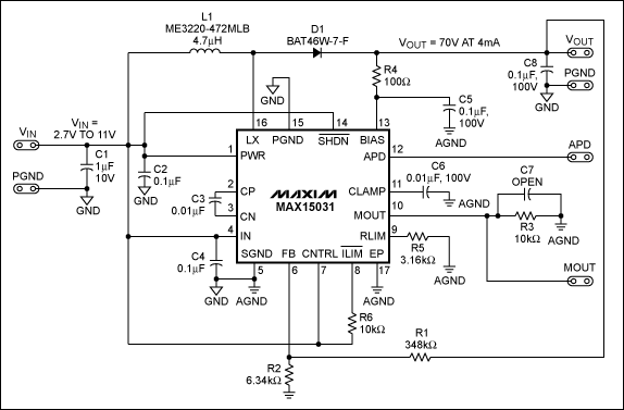
MAX15031应用电路图/MAX15031升压转换器电路原理图
Figure 1 presents the reference design schematic for a 2.7V to 5.5V input range. The same circuit can be used for inputs from 5.5V to 11V by connecting the CP pin to VIN and removing the charge-pump capacitor (C3).
Figure 1. Schematic of the MAX15031 boost converter for FSW = 400kHz (fixed).
