Abstract: Audio application note describes a simple, compact scheme that provides a low noise, low ripple power source for use in audio amplifiers, microphones, headphone amplifiers, CODECs and other audio circuits.
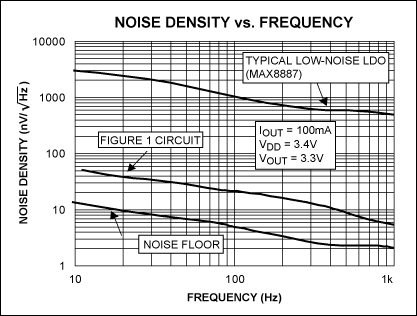
The circuit shown in the figure below reduces noise and ripple voltage by 40dB over the 100Hz to 20kHz audio range. It provides a clean source of 5V power for driving audio circuits in portable applications such as cellular phones and multimedia notebook computers. Most linear regulators reject noise only up to 1000Hz or so, and the bulk of a low-frequency passive filter is unwelcome in portable applications.

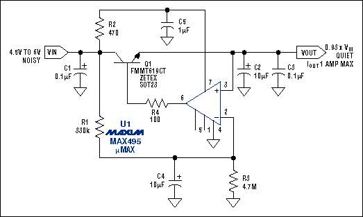
Figure 1. This compact circuit actively compensates for power-supply ripple and noise, providing 40dB of attenuation in the 100Hz to 20kHz audio band.
The circuit shown accepts noisy VCC in the range 4.5V to 6V and produces quiet VCC at a DC level 7% lower. For example, it produces 4.65V at 1A from a nominal 5V source, with only 200µA of quiescent current. The physical layout is very small: one SOT23 transistor, one µMAX (shrink SO-8) op amp, and a few passive components. The largest capacitor is 10µF, and the resistors can be 0.1W or surface-mount 0805 size.
When operating, the circuit acts as a wide-bandwidth buffered voltage follower (not a regulator) whose DC output level is 7% below that of VIN. R1 and R3 form a voltage divider that provides the 7% attenuation, and C4 helps to form a 93% filtered replica of VIN at the op amp's inverting input. The op amp's small input bias current (25nA typical) allows large resistor values for R1 and R3, yet limits the maximum DC error to only 20mV. The result is a lowpass filter with 2Hz corner frequency that provides 20dB of attenuation at 20Hz.
Because the op amp's common-mode input range extends from rail to rail, its noninverting input can sample the output voltage directly. The op amp's supply voltage is filtered by R2 and C5, providing lower output impedance and better power-supply rejection for the op amp at high frequencies. This filter's 300Hz rolloff augments the op amp's PSRR (already impressive at 110dB).
|

Figure 1. This compact circuit actively compensates for power-supply ripple and noise, providing 40dB of attenuation in the 100Hz to 20kHz audio band.
The circuit shown accepts noisy VCC in the range 4.5V to 6V and produces quiet VCC at a DC level 7% lower. For example, it produces 4.65V at 1A from a nominal 5V source, with only 200µA of quiescent current. The physical layout is very small: one SOT23 transistor, one µMAX (shrink SO-8) op amp, and a few passive components. The largest capacitor is 10µF, and the resistors can be 0.1W or surface-mount 0805 size.
When operating, the circuit acts as a wide-bandwidth buffered voltage follower (not a regulator) whose DC output level is 7% below that of VIN. R1 and R3 form a voltage divider that provides the 7% attenuation, and C4 helps to form a 93% filtered replica of VIN at the op amp's inverting input. The op amp's small input bias current (25nA typical) allows large resistor values for R1 and R3, yet limits the maximum DC error to only 20mV. The result is a lowpass filter with 2Hz corner frequency that provides 20dB of attenuation at 20Hz.
Because the op amp's common-mode input range extends from rail to rail, its noninverting input can sample the output voltage directly. The op amp's supply voltage is filtered by R2 and C5, providing lower output impedance and better power-supply rejection for the op amp at high frequencies. This filter's 300Hz rolloff augments the op amp's PSRR (already impressive at 110dB).
A similar article appeared in the January 18, 1996 issue of EDN magazine.
 电子发烧友App











评论