Abstract: This article describes the design of a flyback power converter to operate CCD equipment such as digital cameras from four AAA cells. The MAX752 and a multiple output transformer deliver +15V, -7.5V and 5V. First pass design had low efficiency at low input voltages, and large voltage spikes on the Lx pin. MOSFET operation is improved at low voltage with diodes. Flyback spikes due to non-ideal transformer action are controlled with a snubber network. Efficiency curve shows greater than 80% with a 50-ohm load and 5.25V input. The MAX752 operates at 170kHz. Input voltage range is 3.5V to 6.5V.
A flyback power supply can produce multiple voltages to support products that use charge-coupled devices for imaging.
Products that use charge-coupled devices (CCDs) for imaging require multiple-power-supply voltages, such as 15V, -7.5V, and 5V. A power-supply circuit for generating these voltages has a power source of four AAA alkaline cells and produces an input-voltage range of 3.5V to 6.5V.
The power supply in question is a flyback-transformer type, which operates in a two-step cycle. The first step stores energy in the transformer's primary (acting as an inductor), and the second step transfers energy from the secondaries to the loads. The core of a flyback transformer is selected to store and transfer energy with minimal loss.
Because the heart of a flyback power supply is its transformer, the transformer specifications should be determined early in the design. This gives the transformer vendor adequate time to optimize for size, cost, loss, and temperature rise. In general, you shouldn't undertake the design of a flyback transformer unless you have experience or can afford the time to make a number of iterations. Several items define the transformer:

Figure 1. First pass of flyback power-supply design for battery-powered CCD applications.
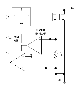
Figure 2. MAX752 internal detail.
To turn on an n-channel MOSFET, you must raise its gate potential above that of the source. On-resistance decreases as the gate voltage increases, so a higher gate voltage raises efficiency by lowering the internal power dissipation. Tests demonstrate, for example, that a low input voltage (3.5V) does not provide sufficient gate voltage for full turn-on of the switching MOSFET in a MAX752. As a solution, D4 and D5 allow the application of a 5.5V supply when the input voltage drops below 4.75V. (See Figure 3.) This technique of powering a DC-DC converter from its output is called "bootstrapping." The higher supply voltage yields better efficiency, as expected.

Figure 3.Final design of the flyback power supply for battery-powered CCD applications.
Heavy output loads cause spikes greater than 20V on the MAX752 Lx pin when the internal MOSFET switches off. These spikes must be corrected, because they exceed the maximum breakdown voltage for the device. The spikes are of very short duration, but they must be understood and suppressed in the interest of long-term reliability.
High-voltage spikes originate in the flyback transformer, whose primary circuit is represented by a simplified model. (See Figure 4.) For clarity, the MOSFET in the MAX752 has been replaced with a simple mechanical switch. Energy is stored in the primary during the first portion of a flyback cycle and transferred from the core through the secondary to the load when S1 opens.

Figure 4. Model of the flyback transformer primary.
An ideal transformer transfers all primary-side energy to the secondary, but the imperfect coupling of an actual transformer allows only a partial transfer. This aberration, modeled as a leakage inductance (Ls), stores energy and produces an inductive "kick" that appears as a brief, high-voltage spike when the power switch opens.
Good transformer design includes bifilar-winding techniques, proper geometry, and correct placement of windings. These measures can minimize, but not eliminate, leakage inductance. You should expect leakage equal to 1% to 2% of the primary inductance and keep in mind that the stored energy is 1/2Lsi 2. The circuit must control this energy while preventing the formation of damaging high voltage.
A circuit called a snubber commonly is included to absorb the energy of the leakage inductance. The simplest snubber (Figure 5) is a resistor across the primary of the flyback transformer. This approach is seldom used, because the resistor constantly wastes energy, gets hot, and lowers the efficiency. A better solution is the series-RC network, whose time constant can be adjusted to provide snubbing for brief intervals only. The RC snubber reduces loss, but it snubs on both the rising and falling edges. What's required is a snubber that operates only on the rising edges.

Figure 5. Snubber circuits for flyback transformers.
A parallel RC network with a series diode forms a snubber that dissipates power only in the rising direction, but designers who are especially concerned about power efficiency may object to wasting the inductive-kick energy in this way. Why not channel the energy and use it? This objective can be met with a small capacitor between primary and secondary. When the primary-side power switch opens, the polarity of voltage across each transformer winding reverses, allowing power to transfer from each secondary to its load. The small capacitor allows the inductive kick to couple across the transformer. Appearing in phase with the secondary's output voltages, this energy quickly passes through each secondary rectifier to the output capacitor.
The curves in the graph below (Figure 6) show slight inflections between 4.5V and 5.0V, as the bootstrap diodes (D4 and D5) shift the IC power from output voltage to input voltage. Because it exhibits poor regulation for secondary outputs not directly sensed by feedback, this flyback design is most appropriate for systems that require tight regulation for one output only. The unregulated outputs move in response to load changes at the main output, but are well regulated against changes in the source voltage. Such "line regulation" is the main concern in battery-operated systems, so this circuit is a good choice for small, efficient, multi-output power supplies.

Figure 6. Efficiency versus supply voltage.
A similar version of this article appeared in the December 1997 issue of Computer Design.
A flyback power supply can produce multiple voltages to support products that use charge-coupled devices for imaging.
Products that use charge-coupled devices (CCDs) for imaging require multiple-power-supply voltages, such as 15V, -7.5V, and 5V. A power-supply circuit for generating these voltages has a power source of four AAA alkaline cells and produces an input-voltage range of 3.5V to 6.5V.
The power supply in question is a flyback-transformer type, which operates in a two-step cycle. The first step stores energy in the transformer's primary (acting as an inductor), and the second step transfers energy from the secondaries to the loads. The core of a flyback transformer is selected to store and transfer energy with minimal loss.
Because the heart of a flyback power supply is its transformer, the transformer specifications should be determined early in the design. This gives the transformer vendor adequate time to optimize for size, cost, loss, and temperature rise. In general, you shouldn't undertake the design of a flyback transformer unless you have experience or can afford the time to make a number of iterations. Several items define the transformer:
- Number of outputs. This design requires 5.5V at 0.1A, 15V at 0.015A, and -7.5V at 0.015A.
- Type of power-conversion IC and its operating frequency. This circuit's MAX752, for example, is a current-mode pulse-width modulator (PWM) operating at 170kHz.
- Type of rectifier used in the secondaries. Low-cost low-current diodes of the 1N4148 type drop about 1V at modest levels of current, and Schottky rectifiers drop about 0.5V at higher levels of current. Either way, the fixed rectifier loss is compensated by the flyback transformer's turns ratio.

Figure 1. First pass of flyback power-supply design for battery-powered CCD applications.

Figure 2. MAX752 internal detail.
To turn on an n-channel MOSFET, you must raise its gate potential above that of the source. On-resistance decreases as the gate voltage increases, so a higher gate voltage raises efficiency by lowering the internal power dissipation. Tests demonstrate, for example, that a low input voltage (3.5V) does not provide sufficient gate voltage for full turn-on of the switching MOSFET in a MAX752. As a solution, D4 and D5 allow the application of a 5.5V supply when the input voltage drops below 4.75V. (See Figure 3.) This technique of powering a DC-DC converter from its output is called "bootstrapping." The higher supply voltage yields better efficiency, as expected.

Figure 3.Final design of the flyback power supply for battery-powered CCD applications.
Heavy output loads cause spikes greater than 20V on the MAX752 Lx pin when the internal MOSFET switches off. These spikes must be corrected, because they exceed the maximum breakdown voltage for the device. The spikes are of very short duration, but they must be understood and suppressed in the interest of long-term reliability.
High-voltage spikes originate in the flyback transformer, whose primary circuit is represented by a simplified model. (See Figure 4.) For clarity, the MOSFET in the MAX752 has been replaced with a simple mechanical switch. Energy is stored in the primary during the first portion of a flyback cycle and transferred from the core through the secondary to the load when S1 opens.

Figure 4. Model of the flyback transformer primary.
An ideal transformer transfers all primary-side energy to the secondary, but the imperfect coupling of an actual transformer allows only a partial transfer. This aberration, modeled as a leakage inductance (Ls), stores energy and produces an inductive "kick" that appears as a brief, high-voltage spike when the power switch opens.
Good transformer design includes bifilar-winding techniques, proper geometry, and correct placement of windings. These measures can minimize, but not eliminate, leakage inductance. You should expect leakage equal to 1% to 2% of the primary inductance and keep in mind that the stored energy is 1/2Lsi 2. The circuit must control this energy while preventing the formation of damaging high voltage.
A circuit called a snubber commonly is included to absorb the energy of the leakage inductance. The simplest snubber (Figure 5) is a resistor across the primary of the flyback transformer. This approach is seldom used, because the resistor constantly wastes energy, gets hot, and lowers the efficiency. A better solution is the series-RC network, whose time constant can be adjusted to provide snubbing for brief intervals only. The RC snubber reduces loss, but it snubs on both the rising and falling edges. What's required is a snubber that operates only on the rising edges.

Figure 5. Snubber circuits for flyback transformers.
A parallel RC network with a series diode forms a snubber that dissipates power only in the rising direction, but designers who are especially concerned about power efficiency may object to wasting the inductive-kick energy in this way. Why not channel the energy and use it? This objective can be met with a small capacitor between primary and secondary. When the primary-side power switch opens, the polarity of voltage across each transformer winding reverses, allowing power to transfer from each secondary to its load. The small capacitor allows the inductive kick to couple across the transformer. Appearing in phase with the secondary's output voltages, this energy quickly passes through each secondary rectifier to the output capacitor.
The curves in the graph below (Figure 6) show slight inflections between 4.5V and 5.0V, as the bootstrap diodes (D4 and D5) shift the IC power from output voltage to input voltage. Because it exhibits poor regulation for secondary outputs not directly sensed by feedback, this flyback design is most appropriate for systems that require tight regulation for one output only. The unregulated outputs move in response to load changes at the main output, but are well regulated against changes in the source voltage. Such "line regulation" is the main concern in battery-operated systems, so this circuit is a good choice for small, efficient, multi-output power supplies.

Figure 6. Efficiency versus supply voltage.
A similar version of this article appeared in the December 1997 issue of Computer Design.
 电子发烧友App







评论