Isolated power supplies have been around since the beginning of the electronics industry. As power-supply designs change to keep pace with increased efficiency and power-density demands, isolated feedback is crucial to maintaining safety.
Isolated power supplies not only protect users from potentially lethal voltages and currents, but they also provide performance benefits. Isolated supplies preserve instrument accuracy by interrupting ground loops, and they easily provide positive regulated voltages from a negative power bus without compromising the benefits of that bus.
Isolated feedback has become more important with advancing technology and with the demands for more efficient regulation and higher power density. Primary-side switching supplies have supplanted secondary-side switching supplies. Also, to improve overall efficiency, linear post-regulators have given way to isolated feedback. Higher frequency operation of switching controllers allows magnetic components to shrink to a fraction of the size of an equivalent-power 60Hz transformer. As a result, designers now depend on isolated feedback to maintain safety at high power densities.
You can use one of three basic techniques to isolate the feedback signal in a power supply. Coupled-winding feedback depends on close coupling between the feedback winding and the output (secondary) winding, and maintains the required isolation between input and output. Optoisolator feedback relies on the linear characteristic of a coupled LED and a phototransistor and the distance between them. Transformer-coupled feedback requires a modulator and a demodulator to transmit the signal through a second transformer.
These techniques assume that a transformer provides the required input-to-output isolation. You can learn about these techniquesby applying each type of isolated feedback to a transformer-flyback topology, which stores energy in the power transformer when the primary switch is on and distributes energy when the switch is off.
You can see an example of isolated coupled-winding feedback by observing the switching-voltage waveform at the primary winding of a transformer-flyback topology (Figure 1a). Assume a positive input voltage and a low-side switch. When the switch closes, its voltage, LX, goes low (Figure 1b), and the primary current, IPRI (Figure 1c), ramps up, storing energy in the transformer.
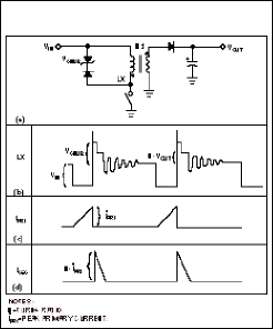
Figure 1. In a simple flyback topology (a) with a positive input voltage and low-side switch, closing the switch pulls the voltage, LX, low (b). The primary current (c) then ramps up, storing energy in the transformer. As the secondary current ramps down (d), power in the transformer transfers to the output.
When the switch opens, LX flies high due to the effect of uncoupled leakage inductance associated with the primary winding. When the energy in this leakage dissipates, usually due to the presence of a diode/zener snubber network, LX settles to a level equal to VIN plus the product of the secondary-winding voltage and the primary-to-secondary turns ratio, N. In other words, LX = VIN+N×VSEC at this point. This level is the isolated-feedback voltage that regulates VOUT.
The feedback voltage remains at VIN+N×VSEC until all of the energy stored in the transformer transfers to the output. LX then settles to VIN. The major disadvantage of this arrangement is the magnitude of the feedback voltage. Offset by VIN and multiplied by the turns ratio, the magnitude becomes impractical at higher levels of VIN.
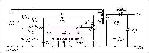
Figure 2. Using only one transformer, a coupled-winding-feedback, +5 to -48V flyback converter can use a bias winding, WFB, to provide an isolated-feedback voltage and to generate a bias supply for the switching controller, IC1.
Deriving feedback from a bias winding is more practical than obtaining feedback from the primary flyback voltage, and the cost is simply that of an extra winding on the transformer. As in the previous example, the output regulation depends on close coupling between the output and feedback windings. This technique is unsuitable for high-power circuits, because cross-regulation limits the load-regulation range.
IC1 regulates the output via pulse-frequency modulation (PFM). PFM regulators turn on the power switch for a fixed interval and vary the frequency of these "on" pulses as necessary to supply the required output power. The advantage of PFM over PWM is PFM's lower power dissipation with light loads. The light-load frequencies are lower, so that the power loss associated with switching is less than that of a comparable fixed-frequency PWM system.
The MOSFET power switch, Q2, controls power into the primary winding, WPRI. Then, power transfers to the output through the secondary winding, WSEC, and the Schottky diode, D3, for storage in C3. The feedback winding, WFB, and D2 supply the power for IC1, which C1 stores. The IC then regulates VOUT by controlling the voltage across C1.
This regulation adjusts the pulse frequency to produce just 12V across the feedback winding. The desired turns ratio from WSEC to WFB is approximately 5 to 12, and these windings must have close coupling to minimize their leakage inductance. Snubber network R4/C2 dissipates energy in the leakage inductance and protects the switch by minimizing the amplitude of flyback spikes.
R3 provides a 25mW preload across the feedback voltage to improve load regulation and stability. R1, R2, D1, and Q1 constitute a startup circuit that provides power to IC1 until the feedback voltage reaches regulation. Once in regulation, the feedback voltage blocks the startup circuit by reverse-biasing the emitter of Q1. The converter in Figure 2 delivers 5V ±4% at 500mA with better than 80% efficiency. Load regulation is approximately 5%, and the line regulation for inputs from -36V to -70V is approximately 0.5%.
At first glance, the optoisolator appears ideal for providing a signal that is isolated from but linearly proportional to the output voltage. An LED emits light whose intensity is proportional to the current through the diode. The light shines across a physical separation to a phototransistor, which conducts current in proportion to the intensity of the light received.
For analog-signal applications, however, the optoisolator, which was originally intended for digital signals, is limited by its own characteristics. The optoisolator's current-transfer ratio is the ratio of output current to input current. This ratio is constant in the ideal case, but in practice it varies with input current, temperature, time, and processing. Over five to 10 years, this ratio can degrade by a factor of 10. Another drawback is that optoisolators are relatively slow. Even the faster ones require input currents of 10mA to 20mA just to maintain their speed. You need to consider all of these factors when designing a practical optoisolated-feedback connection.
A transformer-flyback topology illustrates optoisolated feedback (Figure 3). This circuit converts 12V to an isolated 9V and incorporates a current-mode PFM controller, IC1, which operates with switching frequencies to 300kHz. IC2's shunt regulator, acting as an error amplifier, sinks current when an increasing VOUT pulls the feedback voltage above its internal reference voltage. The optoisolator current increases with this sink current until the converter stops switching, thus allowing VOUT to return to its nominal value.
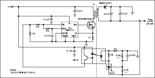
Figure 3. In an optoisolator-feedback flyback design, a transformer isolates the main output, -9V, and an optoisolator isolates the feedback signal.
Placing the error amplifier, IC2, on the secondary side in front of the optoisolator reduces this part's susceptibility to the effects of variation in bias current and temperature. In some circuits, however, the extra gain of this amplifier can compromise loop stability and complicate the loop compensation.
This design uses a high-speed optoisolator (6N136) to provide a wide loop bandwidth and fast transient response. The optoisolator's maximum propagation delay for a 16mA current is 800nsec. In addition, IC1's high switching frequency allows the transformer to be relatively small for its output power. These and other features enable the circuit to meet the Ethernet applications for which it was designed. The circuit derives -9V from 12V with more than 80% efficiency. For supply voltages ranging from 5V to 15V, the circuit services a 200mA load and maintains 0.1% line regulation. Load regulation is better than 0.5% for output currents from 0mA to 200mA, and temperature regulation over -55°C to +125°C varies from 0.97% to 0.57%.
The basic concept is a linearly proportional DC-feedback path with isolation (Figure 4). A push-pull transformer driver, IC2, whose line regulation is zero, generates a transformer-isolated voltage that is proportional to the input. This action enables the switching converter's primary-side error amplifier in IC1 to control the loop as if the circuit had no isolation. Primary transformer T1 provides forward isolation.
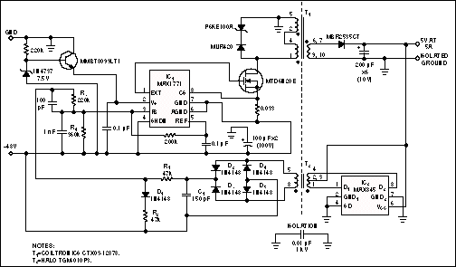
Figure 4. Transformer-coupled feedback uses a separate transformer to allow for the optimum feedback in a -48V to 5V flyback converter. T1 provides forward isolation; T2 isolates the feedback signal.
An isolated transformer driver, IC2, in conjunction with a surface-mount transformer, T2, converts the isolated 5V output to a voltage that is referred to the primary side and proportional to 5V. The diode bridge, D2 to D5, and C1 convert this transformer's output to DC. D1, R1, and R2 compensate for temperature variations in the diode bridge. The resulting voltage has a zero temperature coefficient and is slightly less than one-half the isolated 5V feedback voltage. (IC2 operates on inputs from 3V to 6V.)
The circuit inserts this isolated feedback into the loop of a transformer-flyback switching converter, IC1, which converts -48V to 5V. For 5V outputs, the feedback voltage is 2.404V. At 100kHz, the delay through the feedback circuit, 250nsec, is equal to a 9° phase shift. This frequency is much greater than the loop bandwidth. Supply current for the feedback circuit is approximately 6mA, including the load of the temperature-compensation network.
To accommodate the isolated-feedback circuit, you need only reduce the value of R3 on the nonisolated converter so that the R3/R4 divider voltage matches the 1.5V reference voltage internal to IC1. Note that R3 needs trimming in production to compensate for turns-ratio variations in T2. (For 1% initial tolerance, R3 requires trimming, regardless of the feedback technique.)
The performance of the isolated and nonisolated converters is virtually identical, except for the power consumed by the isolated-feedback circuit. Transformer T2 provides isolation to 500VRMS; ratings to 1500VRMS are also available. The converter delivers an isolated 5V at 5A with efficiency better than 80%. For load currents of 0A to 5A, the load regulation is approximately 2%, and for input voltages of -30V to -65V, the line regulation is less than 1%.
A similar version of this article appeared in the June 19, 1997 issue of EDN.
Isolated power supplies not only protect users from potentially lethal voltages and currents, but they also provide performance benefits. Isolated supplies preserve instrument accuracy by interrupting ground loops, and they easily provide positive regulated voltages from a negative power bus without compromising the benefits of that bus.
Isolated feedback has become more important with advancing technology and with the demands for more efficient regulation and higher power density. Primary-side switching supplies have supplanted secondary-side switching supplies. Also, to improve overall efficiency, linear post-regulators have given way to isolated feedback. Higher frequency operation of switching controllers allows magnetic components to shrink to a fraction of the size of an equivalent-power 60Hz transformer. As a result, designers now depend on isolated feedback to maintain safety at high power densities.
You can use one of three basic techniques to isolate the feedback signal in a power supply. Coupled-winding feedback depends on close coupling between the feedback winding and the output (secondary) winding, and maintains the required isolation between input and output. Optoisolator feedback relies on the linear characteristic of a coupled LED and a phototransistor and the distance between them. Transformer-coupled feedback requires a modulator and a demodulator to transmit the signal through a second transformer.
These techniques assume that a transformer provides the required input-to-output isolation. You can learn about these techniquesby applying each type of isolated feedback to a transformer-flyback topology, which stores energy in the power transformer when the primary switch is on and distributes energy when the switch is off.
Coupled-Winding Feedback
Coupled-winding feedback relies on close coupling between the secondary- and primary-side windings to maintain an accurate image of the output voltage while energy distributes among the windings of the transformer. The main advantage of coupled-winding feedback is its low component count; the power transformer provides the isolation. The main disadvantage is the conflict between the need for close coupling and the need for a high isolation voltage. Another disadvantage is the degradation in cross-regulation that occurs when the current loads are high and unbalanced.You can see an example of isolated coupled-winding feedback by observing the switching-voltage waveform at the primary winding of a transformer-flyback topology (Figure 1a). Assume a positive input voltage and a low-side switch. When the switch closes, its voltage, LX, goes low (Figure 1b), and the primary current, IPRI (Figure 1c), ramps up, storing energy in the transformer.

Figure 1. In a simple flyback topology (a) with a positive input voltage and low-side switch, closing the switch pulls the voltage, LX, low (b). The primary current (c) then ramps up, storing energy in the transformer. As the secondary current ramps down (d), power in the transformer transfers to the output.
When the switch opens, LX flies high due to the effect of uncoupled leakage inductance associated with the primary winding. When the energy in this leakage dissipates, usually due to the presence of a diode/zener snubber network, LX settles to a level equal to VIN plus the product of the secondary-winding voltage and the primary-to-secondary turns ratio, N. In other words, LX = VIN+N×VSEC at this point. This level is the isolated-feedback voltage that regulates VOUT.
The feedback voltage remains at VIN+N×VSEC until all of the energy stored in the transformer transfers to the output. LX then settles to VIN. The major disadvantage of this arrangement is the magnitude of the feedback voltage. Offset by VIN and multiplied by the turns ratio, the magnitude becomes impractical at higher levels of VIN.
Add a Feedback or Bias Winding
A feedback or bias winding provides the second means for obtaining isolated coupled-winding feedback. Consider, for example, a transformer-isolated flyback converter that derives 5V from -48V (Figure 2). The bias winding generates a bias supply for powering the switching controller, provides an isolated-feedback voltage, and level-shifts the feedback signal to allow use of a low-side-referred controller and switch.
Figure 2. Using only one transformer, a coupled-winding-feedback, +5 to -48V flyback converter can use a bias winding, WFB, to provide an isolated-feedback voltage and to generate a bias supply for the switching controller, IC1.
Deriving feedback from a bias winding is more practical than obtaining feedback from the primary flyback voltage, and the cost is simply that of an extra winding on the transformer. As in the previous example, the output regulation depends on close coupling between the output and feedback windings. This technique is unsuitable for high-power circuits, because cross-regulation limits the load-regulation range.
IC1 regulates the output via pulse-frequency modulation (PFM). PFM regulators turn on the power switch for a fixed interval and vary the frequency of these "on" pulses as necessary to supply the required output power. The advantage of PFM over PWM is PFM's lower power dissipation with light loads. The light-load frequencies are lower, so that the power loss associated with switching is less than that of a comparable fixed-frequency PWM system.
The MOSFET power switch, Q2, controls power into the primary winding, WPRI. Then, power transfers to the output through the secondary winding, WSEC, and the Schottky diode, D3, for storage in C3. The feedback winding, WFB, and D2 supply the power for IC1, which C1 stores. The IC then regulates VOUT by controlling the voltage across C1.
This regulation adjusts the pulse frequency to produce just 12V across the feedback winding. The desired turns ratio from WSEC to WFB is approximately 5 to 12, and these windings must have close coupling to minimize their leakage inductance. Snubber network R4/C2 dissipates energy in the leakage inductance and protects the switch by minimizing the amplitude of flyback spikes.
R3 provides a 25mW preload across the feedback voltage to improve load regulation and stability. R1, R2, D1, and Q1 constitute a startup circuit that provides power to IC1 until the feedback voltage reaches regulation. Once in regulation, the feedback voltage blocks the startup circuit by reverse-biasing the emitter of Q1. The converter in Figure 2 delivers 5V ±4% at 500mA with better than 80% efficiency. Load regulation is approximately 5%, and the line regulation for inputs from -36V to -70V is approximately 0.5%.
At first glance, the optoisolator appears ideal for providing a signal that is isolated from but linearly proportional to the output voltage. An LED emits light whose intensity is proportional to the current through the diode. The light shines across a physical separation to a phototransistor, which conducts current in proportion to the intensity of the light received.
For analog-signal applications, however, the optoisolator, which was originally intended for digital signals, is limited by its own characteristics. The optoisolator's current-transfer ratio is the ratio of output current to input current. This ratio is constant in the ideal case, but in practice it varies with input current, temperature, time, and processing. Over five to 10 years, this ratio can degrade by a factor of 10. Another drawback is that optoisolators are relatively slow. Even the faster ones require input currents of 10mA to 20mA just to maintain their speed. You need to consider all of these factors when designing a practical optoisolated-feedback connection.
A transformer-flyback topology illustrates optoisolated feedback (Figure 3). This circuit converts 12V to an isolated 9V and incorporates a current-mode PFM controller, IC1, which operates with switching frequencies to 300kHz. IC2's shunt regulator, acting as an error amplifier, sinks current when an increasing VOUT pulls the feedback voltage above its internal reference voltage. The optoisolator current increases with this sink current until the converter stops switching, thus allowing VOUT to return to its nominal value.

Figure 3. In an optoisolator-feedback flyback design, a transformer isolates the main output, -9V, and an optoisolator isolates the feedback signal.
Placing the error amplifier, IC2, on the secondary side in front of the optoisolator reduces this part's susceptibility to the effects of variation in bias current and temperature. In some circuits, however, the extra gain of this amplifier can compromise loop stability and complicate the loop compensation.
This design uses a high-speed optoisolator (6N136) to provide a wide loop bandwidth and fast transient response. The optoisolator's maximum propagation delay for a 16mA current is 800nsec. In addition, IC1's high switching frequency allows the transformer to be relatively small for its output power. These and other features enable the circuit to meet the Ethernet applications for which it was designed. The circuit derives -9V from 12V with more than 80% efficiency. For supply voltages ranging from 5V to 15V, the circuit services a 200mA load and maintains 0.1% line regulation. Load regulation is better than 0.5% for output currents from 0mA to 200mA, and temperature regulation over -55°C to +125°C varies from 0.97% to 0.57%.
Transformer-Coupled Feedback
Like coupled-winding feedback, transformer-coupled feedback relies on a magnetic field to transmit voltage information across an isolation barrier. Transformer-coupled feedback, however, employs a separate transformer, modulator, and demodulator to allow optimization of the feedback path. The modulator and the demodulator are necessary, because a transformer cannot transmit DC voltage or current. Voltage feedback requires minimal power transfer, so you can increase the modulation frequency with respect to the power-switching frequency and thereby reduce the size of the transformer. Performance depends on the design of the modulator and the transformer; the devil is in the details.The basic concept is a linearly proportional DC-feedback path with isolation (Figure 4). A push-pull transformer driver, IC2, whose line regulation is zero, generates a transformer-isolated voltage that is proportional to the input. This action enables the switching converter's primary-side error amplifier in IC1 to control the loop as if the circuit had no isolation. Primary transformer T1 provides forward isolation.

Figure 4. Transformer-coupled feedback uses a separate transformer to allow for the optimum feedback in a -48V to 5V flyback converter. T1 provides forward isolation; T2 isolates the feedback signal.
An isolated transformer driver, IC2, in conjunction with a surface-mount transformer, T2, converts the isolated 5V output to a voltage that is referred to the primary side and proportional to 5V. The diode bridge, D2 to D5, and C1 convert this transformer's output to DC. D1, R1, and R2 compensate for temperature variations in the diode bridge. The resulting voltage has a zero temperature coefficient and is slightly less than one-half the isolated 5V feedback voltage. (IC2 operates on inputs from 3V to 6V.)
The circuit inserts this isolated feedback into the loop of a transformer-flyback switching converter, IC1, which converts -48V to 5V. For 5V outputs, the feedback voltage is 2.404V. At 100kHz, the delay through the feedback circuit, 250nsec, is equal to a 9° phase shift. This frequency is much greater than the loop bandwidth. Supply current for the feedback circuit is approximately 6mA, including the load of the temperature-compensation network.
To accommodate the isolated-feedback circuit, you need only reduce the value of R3 on the nonisolated converter so that the R3/R4 divider voltage matches the 1.5V reference voltage internal to IC1. Note that R3 needs trimming in production to compensate for turns-ratio variations in T2. (For 1% initial tolerance, R3 requires trimming, regardless of the feedback technique.)
The performance of the isolated and nonisolated converters is virtually identical, except for the power consumed by the isolated-feedback circuit. Transformer T2 provides isolation to 500VRMS; ratings to 1500VRMS are also available. The converter delivers an isolated 5V at 5A with efficiency better than 80%. For load currents of 0A to 5A, the load regulation is approximately 2%, and for input voltages of -30V to -65V, the line regulation is less than 1%.
A similar version of this article appeared in the June 19, 1997 issue of EDN.
 电子发烧友App






评论