A portable system's power supply is a complicated beast. It not only includes numerous sophisticated subsystems for voltage monitoring and power management, it may also generate dual VCC levels (3.3V and 5V) and support the voltage switching required by new PCMCIA cards (Figure 1).

Figure 1. This block diagram shows the power supply in a typical notebook computer, highlighting the key controller ICs.
Other factors add complexity: the constant pressure to miniaturize, the need for increased battery life, and the noise-suppression measures made necessary in portable equipment by internal radio modems and pen digitizers. The result is an unprecedented challenge in power-supply design.
This article discusses the capabilities of a new IC that greatly simplifies power-supply design for notebook computers, handy-terminals, and other portable systems. The chip's sophisticated architecture and high level of integration address many of the main-supply requirements. Their usual order of importance is the following:
Similar considerations apply to power supplies for other portable equipment as well, such as bar-code readers, pH meters, and medical instruments.
Output accuracy is an unsung aspect of the power-supply designer's art. Tight accuracy must be maintained in spite of sharp line transients when the ac adapter is plugged in, and in spite of equally sharp load transients when the computer shifts from suspend mode to run mode. The skilled designer must balance loop gain, loop compensation, switching frequency, and filtering to maintain the required accuracy despite numerous ac and dc perturbations. Cost and efficiency goals, often in conflict with the above, must also be satisfied.
A new buck-regulator IC from Maxim (MAX782) achieves excellent dc accuracy and ac-transient behavior while generating the required output voltages 3.3V, 5V, and 12V (Figure 2). It includes control circuitry for two pulse-width modulated (PWM) buck regulators. Its novel, current-mode PWM control (patent pending) produces a high unity-gain crossover frequency (60kHz) that allows quick recovery from line and load transients-within four or five cycles of the internal 300kHz clock. The new control architecture compares low-level signals directly instead of adding gain first.


Figure 2. These block diagrams show the MAX782 internal functions (a), and details of the SMPS (switch-mode power supply) function (b).
By feeding correctly weighted values of output error, reference voltage, inductor-current ramp, and slope-compensation ramp directly into a proprietary summing comparator, the circuit dispenses with conventional integrating error amplifiers and their associated phase shift and stability problems. This approach also allows the use of smaller filter capacitors.
Another way to reduce filter capacitance is by lowering the PWM loop gain. A deliberately controlled loop gain enables relatively low values of capacitance to establish ac stability, by producing a gain rolloff that reaches unity before the next pole or zero frequency. Setting the initial dc loop gain low allows this gain attenuation to be realized with only 30µF per ampere of load current. The low gain introduces a load-regulation error of about 1.5%, but tight initial accuracy on the output voltages (achieved through laser trimming) holds the overall accuracy to within ±3%.
Another basic concern is the input-voltage range. The low end is determined by the specified minimum battery voltage. At the high end, the regulator must withstand open-circuit output voltages from ac adapters and battery chargers. (The worst-case high voltage usually occurs with batteries removed and ac power applied.) The resulting input-range requirement for 6-cell systems is 6V to 24V. Standard analog-CMOS processes break down at 16V or so, but a new CMOS process from Maxim withstands 30V. Developed specifically for the ICs in battery-powered supplies, it eliminates the need for inelegant hybrid devices and power-hungry bipolar ICs.
During shutdown, when a portable system's load often consists only of static RAM, real-time clock, and power-management logic, the supply current is a few hundred microamps. This current must be supplied either from the backup battery or from the main battery, if present. (Drawing shutdown current from the main battery saves the backup until it's really needed.) Such keep-alive supplies are usually implemented with a linear regulator operating from the main battery.
For the suspend state, in which the main processor runs at a greatly reduced clock rate, the system's supply currents range from 3mA to 10mA. This current range is above the comfort level for linear regulators, so the preferred circuit is a switching regulator with reasonably high efficiency at light loads. The moderate to high currents drawn in the run state, on the other hand, demand the highest possible efficiency (>90%).
A single MAX782 accommodates each of these distinct operating modes. For shutdown operation, the chip includes two low-dropout, micropower linear regulators that maintain 3.3V and 5V outputs while drawing only 70µA of battery current. The critical 3.3V output connects either to the main 3.3V bus or to a separate back-up/keep-alive bus.
For suspend-state operation, the IC brings two circuit innovations to bear. A pulse-skipping mode allows the 3.3V and 5V buck regulators to shift smoothly between variable-frequency operation and the normal fixed-frequency PWM operation. This shift occurs automatically as load currents vary above and below 27% of full load, resulting in optimum efficiency for the regulators. The 5V regulator, for example, is 95% efficient at heavy loads, and more than 80% efficient for load currents ranging from full scale down to 1% of full scale (Figure 3).
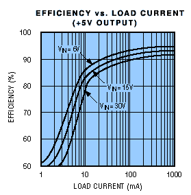
Figure 3. For high currents, the MAX782's 5V output is more than 90% efficient.
Switching noise is unavoidable, but the frequencies and control algorithms employed by the MAX782 insure that the frequency bands of interest for common applications are noise-free. Operation at 300kHz, for instance, leaves a quiet band around the sensitive 455kHz IF of commercial radio (Figure 4a). The harmonics shown (at 300kHz, 600kHz, and 900kHz) remain fixed at those locations as the MAX782's pulse-width modulation responds to changes in load current.
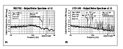
Figure 4. At 1A load currents, the MAX782's 300kHz fixed-frequency PWM control produces no spectral components near the 455kHz IF band (a), but the LT1148's nominal 100kHz variable-frequency control floods that band with noise (b).
The LT1148, on the other hand, is a similar power-controller IC that responds to load-current changes by varying its nominal 100kHz switching frequency. This frequency and its variation combine to fill the 455kHz region with noise (Figure 4b). At lower load currents, the LT1148 maintains regulation by issuing 100kHz pulses in a variable-burst mode whose spectral components contaminate the audio band (Figure 5b). The MAX782 also shifts to variable frequency at low load currents, but at 50mA its 40kHz frequency remains above the audio band (Figure 5a).

Figure 5. At 50mA load currents, both the MAX782 (a) and the LT1148 (b) have switched automatically to variable-frequency operation, but the LT1148's lower frequency contaminates the audio band.
Another MAX782 innovation-fast, precise current sensing-allows the device to turn off its synchronous-rectifier switch as the inductor's discharge current passes through zero. The synchronous rectifier thus continues operating even for light loads, allowing the inductor current to become discontinuous. With both switching regulators operating, the entire 25W MAX782 application circuit draws only 470µA of quiescent battery current.
Competitive chips either disable the synchronous rectifier completely at light loads, or leave it on and pay a big penalty in quiescent supply current. (With the rectifier on, the reversal of inductor current after discharge causes a transfer of energy from the output capacitor back to the battery. Supply current rises because the losses associated with this transfer must be replenished from the battery.)
For run-state operation, the MAX782's balanced design and 300kHz switching frequency provide 95% efficiency without the use of superconductors, solid-gold wires, or large magnetic cores. The circuit's n-channel MOSFET switches and bootstrapped operation enable high efficiency, even with standard surface-mount components (Figure 6).
Figure 6. All components in the MAX782 evaluation kit are surface mount.
Both buck regulators employ logic-level n-channel MOSFETs in place of the p-channel MOSFETs normally used as high-side switches. The n-channel devices' higher majority-carrier mobility results in much lower values of gate capacitance and reverse-transfer capacitance. For devices of equivalent on-resistance, the n-channel types cost 50% less. And for available devices in small SOIC packages, the n-channel parts exhibit only half as much on-resistance.
Gate drive for the high-side MOSFETs is obtained via "bootstrap" capacitors (Figure 7). When the synchronous switch is on, two 0.1µF capacitors (connected to the BST pins) are charged to 5V via two small-signal diodes. Internal switches then turn on either MOSFET by connecting a charged capacitor across gate and source.

Figure 7. The multi-function MAX782 generates high-side gate-drive voltages for the external power MOSFETs.
Start-up power to the MAX782 is delivered by a linear regulator operating on battery voltage. When the 5V output achieves regulation, an internal switchover circuit automatically connects the chip's internal supply rail (via the FB3 pin) to the 5V output. Power for the chip and the gate drivers then comes from the 95%-efficient 5V supply, rather than the inefficient combination of battery and linear regulator. What's more, an adjustable soft-start capability precludes the battery-voltage transients that would otherwise occur each time a buck regulator turns on.
Another efficiency-enhancing feature is the chip's relatively low-voltage threshold for the output-current limit, established by 100mV across a 25mW sense resistor. Other, less-precise designs require a larger drop of 150mV to 200mV across the same resistor, dissipating as much as 400mW in additional power.
When a conventional circuit's high-side switch is on, the flyback circuit stores energy in the inductor core and then discharges a portion of that energy through the secondary winding to the 14V output. During discharge, the primary voltage is VOUT + VSW, where VSW is the synchronous rectifier's saturation voltage. (The secondary output equals the primary output times the turns ratio.) A linear regulator then drops the 14V to 12V.
Unfortunately, if the primary load is removed and the synchronous rectifier turns off at zero current (when no energy is stored), the 14V output in this conventional circuit sags to ground. If the synchronous rectifier remains on, the primary current reverses and the transformer operates in the forward mode. Its output-current capability (theoretically infinite) prevents the 14V output from sagging, but quiescent supply current remains high.
The MAX782, however, achieves excellent cross-regulation with no penalty in quiescent supply current. A second feedback loop in the 5V buck regulator senses the 14V output (VDD). When VDD is in regulation, the rectifier operates normally and turns off at zero current. But if VDD falls below 13V, the loop holds the synchronous rectifier on for an extra microsecond after the primary current reaches zero, causing the transformer to deliver energy in the forward mode (Figure 2b). VDD can therefore deliver hundreds of milliamps, even with the 5V output unloaded.
Another device-the MAX783-derives VPP in the same way, but from 3.3V instead of 5V. It generates VPP with an auxiliary winding on the 3.3V inductor, and regulates VPP via the 3.3V synchronous rectifier. This makes the MAX783 more suitable for systems powered by 6-cell NiCd batteries. Otherwise, the MAX782 and MAX783 are almost identical.
Another cost-saving feature is the inclusion of two linear regulators with outputs switchable to 0V, 5V, or 12V. They provide VPP switching for two memory-card sockets as specified by the PCMCIA memory-card standard. Normally, this switching function is implemented with a 12V supply and a rat's nest of MOSFET switches. The MAX782, however, substitutes two linear-regulator pass transistors for the expensive low-rON MOSFETs. The internal pass transistors are cheap because they occupy little die area.
Decoding logic is also eliminated, because the MAX782 accepts VPP programming code directly from popular PCMCIA controllers such as Intel's 82365SL or Cirrus Logic's CL-PD6720. The MAX782 includes level translators that implement 3.3V/5V PCMCIA switching for VCC. As an alternative, the level translators (which remain alive in the standby mode) can serve as 1%-accurate comparators in circuits that warn of low battery voltage.
The MAX782's high switching frequency (300kHz) lowers the necessary primary inductance to only 10µ-one-fifth of that required in competing IC circuits. The lower inductance means smaller cores, fewer turns, and less power loss in the wire resistance.
The 36-pin monolithic MAX782 also supports miniaturization through its high level of integration, having absorbed the functions of 12V generation, linear regulation, PCMCIA switching, and control for two independent VCC buck regulators. To achieve further size reduction, a shrink small-outline package (SSOP) with tight lead pitch (32 mil) replaces conventional PLCC and SOIC packages.
PDAs and similar devices often include radio modems or RF/electromagnetic-actuated pen-entry digitizers powered directly from the battery. Current switching within the radio can produce voltage ripple, which, reflected from the battery back into the radio, can interfere with the IF signal. As discussed earlier, radio designers are therefore likely to specify suppression of all fundamental and harmonic interference in the vicinity of the IF-near 455kHz, for example.
The MAX782's fixed-frequency PWM architecture provides the predictable frequency spectrum required in such applications. Its free-running oscillator, operating at 200kHz or the pin-strap option of 300kHz, is factory-trimmed to ±10% tolerance and requires no external capacitor.
For demanding applications, you can further reduce noise by synchronizing the internal oscillator to an external clock. Even in its low-power pulse-skipping mode, the MAX782's switching pulses, triggered by the fixed-frequency clock, are more predictable than those of a chaotic burp-mode controller.
The MAX782 has been system-engineered as the main component in portable-system power supplies. One of a family of new power-supply ICs, it leapfrogs the performance of earlier devices by combining high-frequency generation and high efficiency-features that once were mutually exclusive. Other devices in the family are intended either as resonant-mode CCFT/LCD supplies (MAX753/MAX754), or as main supplies for sub-notebook computers (MAX781/MAX782).

Figure 1. This block diagram shows the power supply in a typical notebook computer, highlighting the key controller ICs.
Other factors add complexity: the constant pressure to miniaturize, the need for increased battery life, and the noise-suppression measures made necessary in portable equipment by internal radio modems and pen digitizers. The result is an unprecedented challenge in power-supply design.
This article discusses the capabilities of a new IC that greatly simplifies power-supply design for notebook computers, handy-terminals, and other portable systems. The chip's sophisticated architecture and high level of integration address many of the main-supply requirements. Their usual order of importance is the following:
- Include necessary voltages and functions
- Improve efficiency and extend battery life
- Reduce costs
- Miniaturize
- Minimize EMI (for radios and pen-based computers)
Similar considerations apply to power supplies for other portable equipment as well, such as bar-code readers, pH meters, and medical instruments.
Generate Needed Voltages, with Accuracy
Supply-voltage accuracy is a key requirement in portable systems. Logic-board designers often ask for ±3% accuracy in place of the usual ±5%. And in some applications, these voltages must be slightly offset from the nominal values. Higher voltages compensate for drops across the downstream load switches, and lower voltages extend battery life by minimizing power in the load.Output accuracy is an unsung aspect of the power-supply designer's art. Tight accuracy must be maintained in spite of sharp line transients when the ac adapter is plugged in, and in spite of equally sharp load transients when the computer shifts from suspend mode to run mode. The skilled designer must balance loop gain, loop compensation, switching frequency, and filtering to maintain the required accuracy despite numerous ac and dc perturbations. Cost and efficiency goals, often in conflict with the above, must also be satisfied.
A new buck-regulator IC from Maxim (MAX782) achieves excellent dc accuracy and ac-transient behavior while generating the required output voltages 3.3V, 5V, and 12V (Figure 2). It includes control circuitry for two pulse-width modulated (PWM) buck regulators. Its novel, current-mode PWM control (patent pending) produces a high unity-gain crossover frequency (60kHz) that allows quick recovery from line and load transients-within four or five cycles of the internal 300kHz clock. The new control architecture compares low-level signals directly instead of adding gain first.


Figure 2. These block diagrams show the MAX782 internal functions (a), and details of the SMPS (switch-mode power supply) function (b).
By feeding correctly weighted values of output error, reference voltage, inductor-current ramp, and slope-compensation ramp directly into a proprietary summing comparator, the circuit dispenses with conventional integrating error amplifiers and their associated phase shift and stability problems. This approach also allows the use of smaller filter capacitors.
Another way to reduce filter capacitance is by lowering the PWM loop gain. A deliberately controlled loop gain enables relatively low values of capacitance to establish ac stability, by producing a gain rolloff that reaches unity before the next pole or zero frequency. Setting the initial dc loop gain low allows this gain attenuation to be realized with only 30µF per ampere of load current. The low gain introduces a load-regulation error of about 1.5%, but tight initial accuracy on the output voltages (achieved through laser trimming) holds the overall accuracy to within ±3%.
Another basic concern is the input-voltage range. The low end is determined by the specified minimum battery voltage. At the high end, the regulator must withstand open-circuit output voltages from ac adapters and battery chargers. (The worst-case high voltage usually occurs with batteries removed and ac power applied.) The resulting input-range requirement for 6-cell systems is 6V to 24V. Standard analog-CMOS processes break down at 16V or so, but a new CMOS process from Maxim withstands 30V. Developed specifically for the ICs in battery-powered supplies, it eliminates the need for inelegant hybrid devices and power-hungry bipolar ICs.
Maximum Battery Life
After basic needs are met, the next goal for a portable-system supply is ultra-high efficiency and maximum battery life. But battery life can't be inferred from snapshots of efficiency under fixed load. Instead, you must maximize efficiency over a broad range of load currents, representing shutdown, suspend, and run-state load conditions.During shutdown, when a portable system's load often consists only of static RAM, real-time clock, and power-management logic, the supply current is a few hundred microamps. This current must be supplied either from the backup battery or from the main battery, if present. (Drawing shutdown current from the main battery saves the backup until it's really needed.) Such keep-alive supplies are usually implemented with a linear regulator operating from the main battery.
For the suspend state, in which the main processor runs at a greatly reduced clock rate, the system's supply currents range from 3mA to 10mA. This current range is above the comfort level for linear regulators, so the preferred circuit is a switching regulator with reasonably high efficiency at light loads. The moderate to high currents drawn in the run state, on the other hand, demand the highest possible efficiency (>90%).
A single MAX782 accommodates each of these distinct operating modes. For shutdown operation, the chip includes two low-dropout, micropower linear regulators that maintain 3.3V and 5V outputs while drawing only 70µA of battery current. The critical 3.3V output connects either to the main 3.3V bus or to a separate back-up/keep-alive bus.
For suspend-state operation, the IC brings two circuit innovations to bear. A pulse-skipping mode allows the 3.3V and 5V buck regulators to shift smoothly between variable-frequency operation and the normal fixed-frequency PWM operation. This shift occurs automatically as load currents vary above and below 27% of full load, resulting in optimum efficiency for the regulators. The 5V regulator, for example, is 95% efficient at heavy loads, and more than 80% efficient for load currents ranging from full scale down to 1% of full scale (Figure 3).

Figure 3. For high currents, the MAX782's 5V output is more than 90% efficient.
Switching noise is unavoidable, but the frequencies and control algorithms employed by the MAX782 insure that the frequency bands of interest for common applications are noise-free. Operation at 300kHz, for instance, leaves a quiet band around the sensitive 455kHz IF of commercial radio (Figure 4a). The harmonics shown (at 300kHz, 600kHz, and 900kHz) remain fixed at those locations as the MAX782's pulse-width modulation responds to changes in load current.

Figure 4. At 1A load currents, the MAX782's 300kHz fixed-frequency PWM control produces no spectral components near the 455kHz IF band (a), but the LT1148's nominal 100kHz variable-frequency control floods that band with noise (b).
The LT1148, on the other hand, is a similar power-controller IC that responds to load-current changes by varying its nominal 100kHz switching frequency. This frequency and its variation combine to fill the 455kHz region with noise (Figure 4b). At lower load currents, the LT1148 maintains regulation by issuing 100kHz pulses in a variable-burst mode whose spectral components contaminate the audio band (Figure 5b). The MAX782 also shifts to variable frequency at low load currents, but at 50mA its 40kHz frequency remains above the audio band (Figure 5a).

Figure 5. At 50mA load currents, both the MAX782 (a) and the LT1148 (b) have switched automatically to variable-frequency operation, but the LT1148's lower frequency contaminates the audio band.
Another MAX782 innovation-fast, precise current sensing-allows the device to turn off its synchronous-rectifier switch as the inductor's discharge current passes through zero. The synchronous rectifier thus continues operating even for light loads, allowing the inductor current to become discontinuous. With both switching regulators operating, the entire 25W MAX782 application circuit draws only 470µA of quiescent battery current.
Competitive chips either disable the synchronous rectifier completely at light loads, or leave it on and pay a big penalty in quiescent supply current. (With the rectifier on, the reversal of inductor current after discharge causes a transfer of energy from the output capacitor back to the battery. Supply current rises because the losses associated with this transfer must be replenished from the battery.)
For run-state operation, the MAX782's balanced design and 300kHz switching frequency provide 95% efficiency without the use of superconductors, solid-gold wires, or large magnetic cores. The circuit's n-channel MOSFET switches and bootstrapped operation enable high efficiency, even with standard surface-mount components (Figure 6).
Figure 6. All components in the MAX782 evaluation kit are surface mount.
Both buck regulators employ logic-level n-channel MOSFETs in place of the p-channel MOSFETs normally used as high-side switches. The n-channel devices' higher majority-carrier mobility results in much lower values of gate capacitance and reverse-transfer capacitance. For devices of equivalent on-resistance, the n-channel types cost 50% less. And for available devices in small SOIC packages, the n-channel parts exhibit only half as much on-resistance.
Gate drive for the high-side MOSFETs is obtained via "bootstrap" capacitors (Figure 7). When the synchronous switch is on, two 0.1µF capacitors (connected to the BST pins) are charged to 5V via two small-signal diodes. Internal switches then turn on either MOSFET by connecting a charged capacitor across gate and source.

Figure 7. The multi-function MAX782 generates high-side gate-drive voltages for the external power MOSFETs.
Start-up power to the MAX782 is delivered by a linear regulator operating on battery voltage. When the 5V output achieves regulation, an internal switchover circuit automatically connects the chip's internal supply rail (via the FB3 pin) to the 5V output. Power for the chip and the gate drivers then comes from the 95%-efficient 5V supply, rather than the inefficient combination of battery and linear regulator. What's more, an adjustable soft-start capability precludes the battery-voltage transients that would otherwise occur each time a buck regulator turns on.
Another efficiency-enhancing feature is the chip's relatively low-voltage threshold for the output-current limit, established by 100mV across a 25mW sense resistor. Other, less-precise designs require a larger drop of 150mV to 200mV across the same resistor, dissipating as much as 400mW in additional power.
Cost-Saving Architecture
The next priority in portable-system power supplies is cost reduction. Higher switching frequency in the MAX782 already saves costs through reduced pc area, cheaper magnetic cores, and all-surface-mount construction (which eliminates through-hole assembly steps). The chip's 12V output offers further economy. Derived from an extra winding on the 5V buck inductor, this output is almost free. Though the trick is widely known (it's often called a "coupled-inductor" or "buck with flyback winding" design), the MAX782 circuit's independent 12V regulation provides an extra twist.When a conventional circuit's high-side switch is on, the flyback circuit stores energy in the inductor core and then discharges a portion of that energy through the secondary winding to the 14V output. During discharge, the primary voltage is VOUT + VSW, where VSW is the synchronous rectifier's saturation voltage. (The secondary output equals the primary output times the turns ratio.) A linear regulator then drops the 14V to 12V.
Unfortunately, if the primary load is removed and the synchronous rectifier turns off at zero current (when no energy is stored), the 14V output in this conventional circuit sags to ground. If the synchronous rectifier remains on, the primary current reverses and the transformer operates in the forward mode. Its output-current capability (theoretically infinite) prevents the 14V output from sagging, but quiescent supply current remains high.
The MAX782, however, achieves excellent cross-regulation with no penalty in quiescent supply current. A second feedback loop in the 5V buck regulator senses the 14V output (VDD). When VDD is in regulation, the rectifier operates normally and turns off at zero current. But if VDD falls below 13V, the loop holds the synchronous rectifier on for an extra microsecond after the primary current reaches zero, causing the transformer to deliver energy in the forward mode (Figure 2b). VDD can therefore deliver hundreds of milliamps, even with the 5V output unloaded.
Another device-the MAX783-derives VPP in the same way, but from 3.3V instead of 5V. It generates VPP with an auxiliary winding on the 3.3V inductor, and regulates VPP via the 3.3V synchronous rectifier. This makes the MAX783 more suitable for systems powered by 6-cell NiCd batteries. Otherwise, the MAX782 and MAX783 are almost identical.
Another cost-saving feature is the inclusion of two linear regulators with outputs switchable to 0V, 5V, or 12V. They provide VPP switching for two memory-card sockets as specified by the PCMCIA memory-card standard. Normally, this switching function is implemented with a 12V supply and a rat's nest of MOSFET switches. The MAX782, however, substitutes two linear-regulator pass transistors for the expensive low-rON MOSFETs. The internal pass transistors are cheap because they occupy little die area.
Decoding logic is also eliminated, because the MAX782 accepts VPP programming code directly from popular PCMCIA controllers such as Intel's 82365SL or Cirrus Logic's CL-PD6720. The MAX782 includes level translators that implement 3.3V/5V PCMCIA switching for VCC. As an alternative, the level translators (which remain alive in the standby mode) can serve as 1%-accurate comparators in circuits that warn of low battery voltage.
Miniaturization
Size and weight constraints usually have a slightly lower priority in the design process than does cost. But "creeping featuritis" can be a headache for the power-supply designer, who may be asked at the last minute to supply an extra half ampere, or to confine his circuit to a tiny L-shaped area of pc board.The MAX782's high switching frequency (300kHz) lowers the necessary primary inductance to only 10µ-one-fifth of that required in competing IC circuits. The lower inductance means smaller cores, fewer turns, and less power loss in the wire resistance.
The 36-pin monolithic MAX782 also supports miniaturization through its high level of integration, having absorbed the functions of 12V generation, linear regulation, PCMCIA switching, and control for two independent VCC buck regulators. To achieve further size reduction, a shrink small-outline package (SSOP) with tight lead pitch (32 mil) replaces conventional PLCC and SOIC packages.
Noise and Ripple Reduction
Low-noise/low-EMI power supplies are often required by personal communicators and pen-based personal digital assistants (PDAs). Though poised to scale new heights in personal computing, these devices have yet to prove themselves to the FAA. Supposedly, EMI from a laptop computer was the cause of a recent disruption in the navigation system of an airliner bound for New York.PDAs and similar devices often include radio modems or RF/electromagnetic-actuated pen-entry digitizers powered directly from the battery. Current switching within the radio can produce voltage ripple, which, reflected from the battery back into the radio, can interfere with the IF signal. As discussed earlier, radio designers are therefore likely to specify suppression of all fundamental and harmonic interference in the vicinity of the IF-near 455kHz, for example.
The MAX782's fixed-frequency PWM architecture provides the predictable frequency spectrum required in such applications. Its free-running oscillator, operating at 200kHz or the pin-strap option of 300kHz, is factory-trimmed to ±10% tolerance and requires no external capacitor.
For demanding applications, you can further reduce noise by synchronizing the internal oscillator to an external clock. Even in its low-power pulse-skipping mode, the MAX782's switching pulses, triggered by the fixed-frequency clock, are more predictable than those of a chaotic burp-mode controller.
The MAX782 has been system-engineered as the main component in portable-system power supplies. One of a family of new power-supply ICs, it leapfrogs the performance of earlier devices by combining high-frequency generation and high efficiency-features that once were mutually exclusive. Other devices in the family are intended either as resonant-mode CCFT/LCD supplies (MAX753/MAX754), or as main supplies for sub-notebook computers (MAX781/MAX782).
 电子发烧友App




评论