Abstract: Techniques are described for minimizing power dissipation in linear battery chargers. Beginning with a stable wall-cube switching power source, methods are described to limit the dissipation in the linear charging circuit. Circuits are provided, calculations are shown, heat sinking for the PMOS pass transistor is discussed, and suitable pass transistors are suggested.

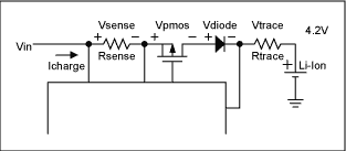
Figure 1. Voltage drop contribution.
Vin = Vsense + Vpmos + Vtrace + Vdiode + 4.2V
The minimum input can be described as below.
Vin(min) = Rsense × Icharge + Rds(on) × Icharge + Rtrace × Icharge + (Vthmax(d) + Rd × Icharge) + 4.2V
Where Vdiode = Vthmax(d) + Rd × Icharge, Vthmax(d); Diode turn on threshold voltage, Rd; Diode series resistance
As we see in the above equation, the charger requires higher input voltage if the charge current (Icharge) is increased. Below is actual data from an example circuit (Figure 4) when the charge current is 500mA.
Vin = 0.303V(Vdiode) + 0.060V(Vsense) + 0.112V(Vpmos) + 0.000V(Vtrace) + 4.2V
Vin = 4.68V
Schottky diode: Zetex ZHCS1000,
PMOS FET: Fairchild FDC636P,
Rsense = 105mΩ,
Rtrace: 40mils wide, 0.5" long, and 1 oz copper trace. This value depends upon PCB layout and battery contacts.
Since this data was taken from one prototype, we should also consider the tolerances of each parameter. A 5V±5% well-regulated switching mode AC adapter will provide some margin, to account for tolerances. The AC adapter does not need an accurate current limit since the charger has a current control, but the AC adapter maximum current capability must be 200-300mA higher than the fast charge current of the linear charger. Figure 2 shows an example of an AC adapter using a MAX5021 low-power, current-mode PWM controller.

Figure 2. 5V/1A AC adapter.

Figure 3. The MAX1898 single-cell Li+ linear charger.
Total power dissipation for the linear charger can be expressed as below.
Pdiss = (Vin - Vbatt) × Icharge
To decide the fast charging current, we need to calculate the worst-case allowable power dissipation on the P-MOSFET Q1.
Power dissipation on the Q1 is expressed as below:
Pdiss(Q1) = Vds(Q1) × Icharge
Vds(Q1) = 5V - VD1 - Icharge × Rcs - Vbatt
Where VD1: D1 forward voltage drop, Rcs: internal current sensing resistor.
Also, the junction temperature of the P-MOSFET should not exceed its maximum limit = 150°C at any operating conditions.
Tj = Ta + RΘJA × Pdiss(Q1)
Table 1 shows some possible P-MOSFET products that can be used in the charger. Even though the specifications show quite high maximum power dissipations, we should be cautious of the PCB mount condition. The "1 in_ pad of 2oz Cu on FR-4 board" specified for package rating on many MOSFET devices may not be realistic for many applications. Instead, the following design procedure yields more practical results.
Table 1.
At first, we should figure out the best RΘJA that we could get given the system design restrictions. The RΘJA is the sum of the junction-to-case (RΘJC) and case-to-ambient thermal resistance (RΘCA), where the case thermal reference is defined as the solder mounting surface of the drain pins. RΘJC is guaranteed by design, while RΘCA is determined by the user's board design, heatsinking method, and a cooling system. We should reduce the RΘCA as low as possible. However, there will be some restrictions such as a limited board space, no ventilation, and safety requirements for PCB material. Since we cannot measure the Tj directly, we can use Tc to compute RΘCA.
Tc = Ta + RΘCA × Pdiss(Q1)
RΘCA = (Tc - Ta)/ Pdiss(Q1)
To design an efficient heatsink for a surface mount PMOS FET, we should increase the drain pin board areas as much as we can. And then we can measure the Vd-s (Q1), Icharge, and Tc to calculate RΘCA. If the measured RΘCA is lower than what we expect, we should increase the surface area of the drain pin pads or reduce the charge current. Also, we should keep in mind that Tc must not exceed 130°C or 150°C PCB maximum operating temperature, depending upon PCB materials. We should check UL file numbers of PCB material that we use and their maximum operating temperature before we start. Let's assume we are using FR-4 two layer boards rated at 130°C max.
If the measured case temperature Tc is 125°C at Ta = 50°C and Pdiss(Q1) = 800mW,
125°C = 50°C + RΘCAx800mW
RΘCA = (125°C - 50°C)/0.8W
= 93.75°C/W
If RΘCA = 93.75°C/W, RΘCJ = 30°C/W (TSOP-6), Ta(max)= 50°C, and Tj(max) = 150°C, the maximum power dissipation that we can achieve;
150°C = 50°C + 123.75°C/W × Pdiss(Q1)
Pdiss(Q1)max = 808mW
If the initial Vbatt = 3.0V, Rcs = 105mΩ, and VD1 = 0.35V at Icharge = 500mA, the worst case Vds(Q1) max is;
Vds(Q1)max = 5V - VD1 - Icharge × Rcs - Vbatt = 1.40V
The allowable maximum charge current is:
Icharge(max) = Poises(Q1)max/Vds(Q1)max
= 808mW/1.60V
= 505mA
Of course, the power dissipation will gradually drop as the battery voltage rises.
Introduction
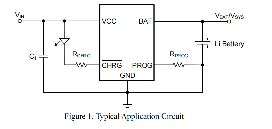
Data sheets for single-cell Li+ linear chargers seldom discuss power dissipation or how to deal with heat dissipation. High input voltage and charge current increase the amount of power the pass element must handle. This application note discusses how to maximize charging current while maintaining safe device and system temperature limits.Use a Proper DC Input Source
A low voltage input reduces the power dissipation. In order to charge the single-cell Li+ battery, we need a well regulated 4.2V±1% or 4.1V±1% (depending on battery chemistry) output. The input voltage needs to be higher to cover the voltage drops between the battery positive terminal and the input DC source. Figure 1 shows these for a typical charger.
Figure 1. Voltage drop contribution.
Vin = Vsense + Vpmos + Vtrace + Vdiode + 4.2V
The minimum input can be described as below.
Vin(min) = Rsense × Icharge + Rds(on) × Icharge + Rtrace × Icharge + (Vthmax(d) + Rd × Icharge) + 4.2V
Where Vdiode = Vthmax(d) + Rd × Icharge, Vthmax(d); Diode turn on threshold voltage, Rd; Diode series resistance
As we see in the above equation, the charger requires higher input voltage if the charge current (Icharge) is increased. Below is actual data from an example circuit (Figure 4) when the charge current is 500mA.
Vin = 0.303V(Vdiode) + 0.060V(Vsense) + 0.112V(Vpmos) + 0.000V(Vtrace) + 4.2V
Vin = 4.68V
Schottky diode: Zetex ZHCS1000,
PMOS FET: Fairchild FDC636P,
Rsense = 105mΩ,
Rtrace: 40mils wide, 0.5" long, and 1 oz copper trace. This value depends upon PCB layout and battery contacts.
Since this data was taken from one prototype, we should also consider the tolerances of each parameter. A 5V±5% well-regulated switching mode AC adapter will provide some margin, to account for tolerances. The AC adapter does not need an accurate current limit since the charger has a current control, but the AC adapter maximum current capability must be 200-300mA higher than the fast charge current of the linear charger. Figure 2 shows an example of an AC adapter using a MAX5021 low-power, current-mode PWM controller.

Figure 2. 5V/1A AC adapter.
Optimize Charge Current and Power Dissipation
Figure 3 shows the circuit used for testing. It is a linear charger with a 500mA charge current and a 6 hours timer limit.
Figure 3. The MAX1898 single-cell Li+ linear charger.
Total power dissipation for the linear charger can be expressed as below.
Pdiss = (Vin - Vbatt) × Icharge
To decide the fast charging current, we need to calculate the worst-case allowable power dissipation on the P-MOSFET Q1.
Power dissipation on the Q1 is expressed as below:
Pdiss(Q1) = Vds(Q1) × Icharge
Vds(Q1) = 5V - VD1 - Icharge × Rcs - Vbatt
Where VD1: D1 forward voltage drop, Rcs: internal current sensing resistor.
Also, the junction temperature of the P-MOSFET should not exceed its maximum limit = 150°C at any operating conditions.
Tj = Ta + RΘJA × Pdiss(Q1)
Table 1 shows some possible P-MOSFET products that can be used in the charger. Even though the specifications show quite high maximum power dissipations, we should be cautious of the PCB mount condition. The "1 in_ pad of 2oz Cu on FR-4 board" specified for package rating on many MOSFET devices may not be realistic for many applications. Instead, the following design procedure yields more practical results.
Table 1.
|
Package |
Pd, Maximum Power Dissipation |
RΘJA, RΘJC, RΘCA Thermal Resistance |
PCB Mount | |
|
FDC636P |
|
|
RΘJC= 30°C/W RΘCA= 48°C/W |
|
|
0.417W at 85°C |
RΘJC= 30°C/W RΘCA= 126°C/W |
|
||
|
Si3441DV |
|
|
RΘJC= 30°C/W RΘCA= 80°C/W |
|
|
|
||||
|
Si5443DC |
|
|
RΘJC= 20°C/W RΘCA= 75°C/W |
|
At first, we should figure out the best RΘJA that we could get given the system design restrictions. The RΘJA is the sum of the junction-to-case (RΘJC) and case-to-ambient thermal resistance (RΘCA), where the case thermal reference is defined as the solder mounting surface of the drain pins. RΘJC is guaranteed by design, while RΘCA is determined by the user's board design, heatsinking method, and a cooling system. We should reduce the RΘCA as low as possible. However, there will be some restrictions such as a limited board space, no ventilation, and safety requirements for PCB material. Since we cannot measure the Tj directly, we can use Tc to compute RΘCA.
Tc = Ta + RΘCA × Pdiss(Q1)
RΘCA = (Tc - Ta)/ Pdiss(Q1)
To design an efficient heatsink for a surface mount PMOS FET, we should increase the drain pin board areas as much as we can. And then we can measure the Vd-s (Q1), Icharge, and Tc to calculate RΘCA. If the measured RΘCA is lower than what we expect, we should increase the surface area of the drain pin pads or reduce the charge current. Also, we should keep in mind that Tc must not exceed 130°C or 150°C PCB maximum operating temperature, depending upon PCB materials. We should check UL file numbers of PCB material that we use and their maximum operating temperature before we start. Let's assume we are using FR-4 two layer boards rated at 130°C max.
If the measured case temperature Tc is 125°C at Ta = 50°C and Pdiss(Q1) = 800mW,
125°C = 50°C + RΘCAx800mW
RΘCA = (125°C - 50°C)/0.8W
= 93.75°C/W
If RΘCA = 93.75°C/W, RΘCJ = 30°C/W (TSOP-6), Ta(max)= 50°C, and Tj(max) = 150°C, the maximum power dissipation that we can achieve;
150°C = 50°C + 123.75°C/W × Pdiss(Q1)
Pdiss(Q1)max = 808mW
If the initial Vbatt = 3.0V, Rcs = 105mΩ, and VD1 = 0.35V at Icharge = 500mA, the worst case Vds(Q1) max is;
Vds(Q1)max = 5V - VD1 - Icharge × Rcs - Vbatt = 1.40V
The allowable maximum charge current is:
Icharge(max) = Poises(Q1)max/Vds(Q1)max
= 808mW/1.60V
= 505mA
Of course, the power dissipation will gradually drop as the battery voltage rises.
 电子发烧友App






评论