Abstract: A boost DC-DC controller built with the MAX1771 DC-DC controller makes a simple switch-mode current source that is useful for battery charging. The voltage control loop is disabled so that the current control loop provides regulation.
The switching regulator of Figure 1 includes independent loops of current and voltage feedback for maintaining regulation. By disabling the voltage loop, you can use the current loop to implement a general-purpose current source.
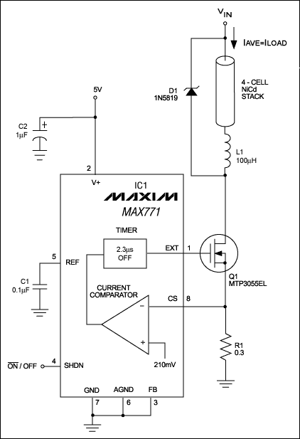
Figure 1. The connections shown convert this switch-mode voltage regulator to a general-purpose current source.
First, apply 5V to V+. Because the chip expects 12V of feedback at that terminal, it assumes a loss of regulation and shifts control to the current loop. This mode of operation allows an increasing ramp of current through Q1, causing the voltage at CS (pin 8) to increase until it reaches the internal comparator threshold (210mV). Timing circuitry then turns off Q1 for a fixed 2.3µs, and the cycle repeats. The result is a relatively constant inductor current, which is also the load current (Figure 2.)

Figure 2. The gate drive for Q1 and the resulting current through L1 are related as shown.
With the proper component values, the circuit generates constant current over a wide range of input voltages. The Figure 1 circuit (with component values shown) is a fast charger for NiCd batteries that provides 600mA charging currents. Calculations are as follows:
The peak inductor current is IPEAK = VSENSE/R1, where VSENSE is the 210mV threshold of the current-sense comparator. The dither current (peak-to-peak value of the ac component of load current) is:
(1) IDITHER = VBATT tOFF/L,
where VBATT is the battery voltage, tOFF is the 2.3µs interval mentioned earlier, and L is the inductance of L1.
As illustrated in Figure 2, the average inductor current is IAVE = IPEAK - ½IDITHER. Substituting from above,

First, choose an average current for the proposed current source (600mA in this circuit). Next, determine the nominal value of VBATT (4.8V in this case). Next, to ensure a relatively small ac (vs. dc) component, set the dither current in equation 1 less than 0.2IAVE and solve for L:

(Use L = 100µH.)
Next, plug this L value (100µH) into equation 2 and solve for R1:

(Use R1 = 300mΩ.)
Three forms of error cause IAVE to deviate from the specified 600mA (Figure 3): variations in VSENSE, delay through the comparator and MOSFET (Q1), and tolerance on the current-sense resistor R1. At lower voltages, the largest error is that of VSENSE, specified in the IC1 data sheet as 210mV ±30mV or about 14%. (In this circuit the value was about 190mV.)

Figure 3. Current-source errors increase with input voltage, as explained in the text.
At higher voltages, delays cause the peak current to overshoot the current limit. You can minimize this error by choosing the inductor value as follows:
(5) L (in µH) > 5.5 (VIN VBATT),
with VIN and VBATT in volts.
Other error sources-the variations in VBATT, tOFF, and L-are relatively small because they relate to IDITHER, which is limited to a small fraction of IAVE.
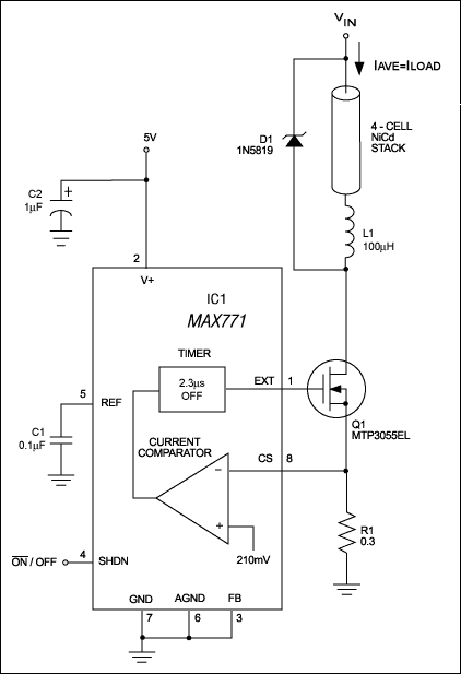
The switching regulator of Figure 1 includes independent loops of current and voltage feedback for maintaining regulation. By disabling the voltage loop, you can use the current loop to implement a general-purpose current source.

Figure 1. The connections shown convert this switch-mode voltage regulator to a general-purpose current source.
First, apply 5V to V+. Because the chip expects 12V of feedback at that terminal, it assumes a loss of regulation and shifts control to the current loop. This mode of operation allows an increasing ramp of current through Q1, causing the voltage at CS (pin 8) to increase until it reaches the internal comparator threshold (210mV). Timing circuitry then turns off Q1 for a fixed 2.3µs, and the cycle repeats. The result is a relatively constant inductor current, which is also the load current (Figure 2.)

Figure 2. The gate drive for Q1 and the resulting current through L1 are related as shown.
With the proper component values, the circuit generates constant current over a wide range of input voltages. The Figure 1 circuit (with component values shown) is a fast charger for NiCd batteries that provides 600mA charging currents. Calculations are as follows:
The peak inductor current is IPEAK = VSENSE/R1, where VSENSE is the 210mV threshold of the current-sense comparator. The dither current (peak-to-peak value of the ac component of load current) is:
(1) IDITHER = VBATT tOFF/L,
where VBATT is the battery voltage, tOFF is the 2.3µs interval mentioned earlier, and L is the inductance of L1.
As illustrated in Figure 2, the average inductor current is IAVE = IPEAK - ½IDITHER. Substituting from above,

First, choose an average current for the proposed current source (600mA in this circuit). Next, determine the nominal value of VBATT (4.8V in this case). Next, to ensure a relatively small ac (vs. dc) component, set the dither current in equation 1 less than 0.2IAVE and solve for L:

(Use L = 100µH.)
Next, plug this L value (100µH) into equation 2 and solve for R1:

(Use R1 = 300mΩ.)
Three forms of error cause IAVE to deviate from the specified 600mA (Figure 3): variations in VSENSE, delay through the comparator and MOSFET (Q1), and tolerance on the current-sense resistor R1. At lower voltages, the largest error is that of VSENSE, specified in the IC1 data sheet as 210mV ±30mV or about 14%. (In this circuit the value was about 190mV.)

Figure 3. Current-source errors increase with input voltage, as explained in the text.
At higher voltages, delays cause the peak current to overshoot the current limit. You can minimize this error by choosing the inductor value as follows:
(5) L (in µH) > 5.5 (VIN VBATT),
with VIN and VBATT in volts.
Other error sources-the variations in VBATT, tOFF, and L-are relatively small because they relate to IDITHER, which is limited to a small fraction of IAVE.
 电子发烧友App





评论