Abstract: This application note presents to the reader a recommended Li-Ion battery pack circuit design for using Dallas Semiconductor 1-Wire® products with low-side N-channel safety FETs. Critical design considerations concerning the placement of the devices in the pack with respect to each other and the battery cell as well as ESD protection are the focus of the text. The reference design illustrates the proper layout implementation and necessary external components needed to avoid possible unsafe operation of a battery pack containing a Dallas Semiconductor 1-Wire device.

Figure 1. Potential charging path that bypasses safety FETs if Dallas chip is on the cell side of the FETs.
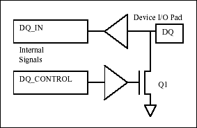
The drain-to-body diode of the n-channel open-drain DQ output driver of the Dallas chip could provide a charging path (highlighted in Figure 1) through the device that will bypass the protection FETs. This conduction path will exist only if the potential difference between VCH and ΦpDQ is more than a diode drop greater than the sum of VCELL and the voltage drop across R1. While such a condition is unlikely, it does illustrate a possible way to bypass the safety circuit if the Dallas chip is connected on the cell side of the safety FETs. Dallas thus recommends connecting the Dallas battery management device on the terminal side of the safety FETs, unless otherwise recommended by the Li+ cell manufacturer.

Figure 2. Recommended schematic for single-cell Li+ pack with low-side n-channel protection FETs.
Overview
Dallas' 1-Wire battery management products are designed with the strategy to minimize electronics in the battery pack while utilizing host-system resources whenever possible to minimize battery pack cost. The hardware design of a Dallas-based battery pack is quite simple, with very few external components required. This application note addresses the implementation of a Dallas-based Li-Ion (Li+) battery pack with low-side n-channel safety FETs. A reference design using the DS18B20 1-Wire digital thermometer is presented focusing on Li+ cell safety and ESD-hardness. This application note also applies to the DS1820 and DS1822 devices.Li+ Safety Considerations
Safety will be considered first. Dallas recommends that no circuit should exist on the Li+ cell side of the safety FETs. Such a connection could compromise overall safety of the battery pack by potentially bypassing the safety FETs. An example of such a case is illustrated in Figure 1.
Figure 1. Potential charging path that bypasses safety FETs if Dallas chip is on the cell side of the FETs.
The drain-to-body diode of the n-channel open-drain DQ output driver of the Dallas chip could provide a charging path (highlighted in Figure 1) through the device that will bypass the protection FETs. This conduction path will exist only if the potential difference between VCH and ΦpDQ is more than a diode drop greater than the sum of VCELL and the voltage drop across R1. While such a condition is unlikely, it does illustrate a possible way to bypass the safety circuit if the Dallas chip is connected on the cell side of the safety FETs. Dallas thus recommends connecting the Dallas battery management device on the terminal side of the safety FETs, unless otherwise recommended by the Li+ cell manufacturer.
Dallas Reference Design
Figure 2 below illustrates the recommended implementation of the Dallas DS18B20 with respect to the low-side n-channel safety FETs. Additionally, Dallas recommends passive devices that primarily serve to protect the DS18B20 from ESD damage or a latchup state resulting from ESD. The protection offered by each device is described below:
Figure 2. Recommended schematic for single-cell Li+ pack with low-side n-channel protection FETs.
- The capacitor C1 on VCC is simply a high-frequency bypass cap. 0.1 µgF is recommended.
- The 5.1V Zener D1 on VCC serves two purposes. It clamps at the Zener voltage of 5.1V so that excessive DC voltage, ESD, and switching transients cannot damage the DS18B20 through VCC. In the forward bias region, it clamps around 0.7V, thereby disallowing VCC from falling more than 0.7V below GND, which is possible when both the CHarge and DIScharge FETs are high impedance.
- The resistor R1 in series with DQ limits current through the large ESD protection diode internally connected between DQ and GND and through the external protection diode D2. R1 > 470Ω is recommended, but consider the size of the pullup on DQ (which is generally installed in the host system) and the DQ I/O specs before setting this value.
- The resistor R2 in series with VCC limits current so that ESD-induced latchup cannot occur. R2 > 270Ω is recommended, and should have very little effect on supply voltage at the DS18B20 max spec. current of 1.5mA. In choosing R2, also consider the power dissipation via R2 and D1 if your application allows the Pack+ (P+) voltage to reach well above the Zener clamp voltage.
- The Zener diode D2 performs the same function for DQ as D1 does for VCC. Choose a Zener value larger than the communication logic-high level for the application, but lower than the 5.5V maximum rating for DQ. A 5.1V Zener diode is recommended.
1-Wire is a registered trademark of Maxim Integrated Products, Inc.
 电子发烧友App














评论