描述
OMAP3530和OMAP3525器件基于增强型OMAP 3架构。
OMAP 3架构旨在提供最佳的OMAP 3架构。类视频,图像和图形处理足以支持以下内容:
该设备支持高级操作系统(HLOS),例如:
-
Linux®
-
Windows®CE
< li> Android™
此OMAP设备包含高性能移动产品所需的最先进的电源管理技术。
以下子系统是其中的一部分设备:
-
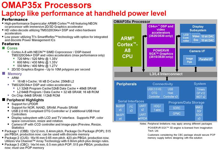
基于ARM Cortex-A8微处理器的微处理器单元(MPU)子系统
-
带有C64x +数字信号处理器(DSP)内核的IVA2.2子系统< /li>
-
用于支持显示的3D图形加速的PowerVR SGX子系统(仅限OMAP3530设备)
-
支持相机图像信号处理器(ISP)端口多种格式和连接到各种图像传感器的接口选项
-
显示子系统具有多种并发图像处理功能,以及支持各种显示器的可编程接口。显示子系统还支持NTSC和PAL视频输出。
-
3级(L3)和4级(L4)互连,为多个启动器提供高带宽数据传输到内部和外部存储器控制器以及打开芯片外设
该器件还提供:
-
全面的电源和时钟管理方案,可实现高性能,低功耗运行,以及超低功耗待机功能。该器件还支持SmartReflex自适应电压控制。这种用于自动控制模块工作电压的电源管理技术可降低有功功耗。
-
使用封装上封装(POP)实现的存储器堆叠功能(仅限CBB和CBC封装)
OMAP3530和OMAP3525器件采用515引脚s-PBGA封装(CBB后缀),515引脚s-PBGA封装(CBC后缀)和423引脚s- PBGA封装(CUS后缀)。 CUS包中没有CBB和CBC包的某些功能。 (有关封装差异,请参见表1-1)。
本数据手册介绍了OMAP3530和OMAP3525应用处理器的电气和机械规格。除非另有说明,否则本数据手册中的信息适用于OMAP3530和OMAP3525应用处理器的商用和扩展温度版本。本数据手册由以下部分组成:
-
第2节:端子描述:分配,电气特性,多路复用和功能描述
-
第3节:电气特性:电源域,工作条件,功耗和直流特性
-
第4节:时钟规范输入和输出时钟,DPLL和DLL
-
第5节:视频Dac规范
-
第6节:时序要求和开关特性
-
第7节:封装特性:可用封装的热特性,器件命名和机械数据
特性
-
OMAP3530 and OMAP3525 Devices:
-
OMAP™ 3 Architecture
-
MPU Subsystem
-
Up to 720-MHz ARM® Cortex™-A8 Core
-
NEON™ SIMD Coprocessor
-
High-Performance Image, Video, Audio (IVA2.2™) Accelerator Subsystem
-
Up to 520-MHz TMS320C64x+™ DSP Core
-
Enhanced Direct Memory Access (EDMA) Controller (128 Independent Channels)
-
Video Hardware Accelerators
-
PowerVR® SGX™ Graphics Accelerator (OMAP3530 Device Only)
-
Tile-Based Architecture Delivering up to 10 MPoly/sec
-
Universal Scalable Shader Engine: Multi-threaded Engine Incorporating Pixel and Vertex Shader Functionality
-
Industry Standard API Support: OpenGLES 1.1 and 2.0, OpenVG1.0
-
Fine-Grained Task Switching, Load Balancing, and Power Management
-
Programmable High-Quality Image Anti-Aliasing
-
Fully Software-Compatible with C64x and ARM9™
-
Commercial and Extended Temperature Grades
-
Advanced Very-Long-Instruction-Word (VLIW) TMS320C64x+ DSP Core
-
Eight Highly Independent Functional Units
-
Six ALUs (32- and 40-Bit), Each Supports Single 32-Bit, Dual 16-Bit, or Quad 8-Bit Arithmetic per Clock Cycle
-
Two Multipliers Support Four 16 x 16-Bit Multiplies (32-Bit Results) per Clock Cycle or Eight 8 x 8-Bit Multiplies (16-Bit Results) per Clock Cycle
-
Load-Store Architecture with Nonaligned Support
-
64 32-Bit General-Purpose Registers
-
Instruction Packing Reduces Code Size
-
All Instructions Conditional
-
Additional C64x+ Enhancements
-
Protected Mode Operation
-
Exceptions Support for Error Detection and Program Redirection
-
Hardware Support for Modulo Loop Operation
-
C64x+ L1 and L2 Memory Architecture
-
32KB of L1P Program RAM and Cache (Direct Mapped)
-
80KB of L1D Data RAM and Cache (2-Way Set-Associative)
-
64KB of L2 Unified Mapped RAM and Cache (4-Way Set-Associative)
-
32KB of L2 Shared SRAM and 16KB of L2 ROM
-
C64x+ Instruction Set Features
-
Byte-Addressable (8-, 16-, 32-, and 64-Bit Data)
-
8-Bit Overflow Protection
-
Bit Field Extract, Set, Clear
-
Normalization, Saturation, Bit-Counting
-
Compact 16-Bit Instructions
-
Additional Instructions to Support Complex Multiplies
-
ARM Cortex-A8 Core
-
ARMv7 Architecture
-
TrustZone®
-
Thumb®-2
-
MMU Enhancements
-
In-Order, Dual-Issue, Superscalar Microprocessor Core
-
NEON Multimedia Architecture
-
Over 2x Performance of ARMv6 SIMD
-
Supports Both Integer and Floating-Point SIMD
-
Jazelle® RCT Execution Environment Architecture
-
Dynamic Branch Prediction with Branch Target Address Cache, Global History Buffer, and 8-Entry Return Stack
-
Embedded Trace Macrocell (ETM) Support for Noninvasive Debug
-
ARM Cortex-A8 Memory Architecture:
-
16-KB Instruction Cache (4-Way Set-Associative)
-
16-KB Data Cache (4-Way Set-Associative)
-
256-KB L2 Cache
-
112KB of ROM
-
64KB of Shared SRAM
-
Endianess:
-
ARM Instructions – Little Endian
-
ARM Data – Configurable
-
DSP Instruction and Data - Little Endian
-
External Memory Interfaces:
-
SDRAM Controller (SDRC)
-
16- and 32-Bit Memory Controller with 1GB of Total Address Space
-
Interfaces to Low-Power Double Data Rate (LPDDR) SDRAM
-
SDRAM Memory Scheduler (SMS) and Rotation Engine
-
General Purpose Memory Controller (GPMC)
-
16-Bit-Wide Multiplexed Address and Data Bus
-
Up to 8 Chip-Select Pins with 128-MB Address Space per Chip-Select Pin
-
Glueless Interface to NOR Flash, NAND Flash (with ECC Hamming Code Calculation), SRAM, and Pseudo-SRAM
-
Flexible Asynchronous Protocol Control for Interface to Custom Logic (FPGA, CPLD, ASICs, and so forth)
-
Nonmultiplexed Address and Data Mode (Limited 2-KB Address Space)
-
System Direct Memory Access (sDMA) Controller (32 Logical Channels with Configurable Priority)
-
Camera Image Signal Processor (ISP)
-
CCD and CMOS Imager Interface
-
Memory Data Input
-
BT.601 (8-Bit) and BT.656 (10-Bit) Digital YCbCr 4:2:2 Interface
-
Glueless Interface to Common Video Decoders
-
Resize Engine
-
Resize Images From 1/4x to 4x
-
Separate Horizontal and Vertical Control
-
Display Subsystem
-
Parallel Digital Output
-
Up to 24-Bit RGB
-
HD Maximum Resolution
-
Supports Up to 2 LCD Panels
-
Support for Remote Frame Buffer Interface (RFBI) LCD Panels
-
2 10-Bit Digital-to-Analog Converters (DACs) Supporting:
-
Composite NTSC and PAL Video
-
Luma and Chroma Separate Video (S-Video)
-
Rotation 90-, 180-, and 270-Degrees
-
Resize Images From 1/4x to 8x
-
Color Space Converter
-
8-Bit Alpha Blending
-
Serial Communication
-
5 Multichannel Buffered Serial Ports (McBSPs)
-
512-Byte Transmit and Receive Buffer (McBSP1, McBSP3, McBSP4, and McBSP5)
-
5-KB Transmit and Receive Buffer (McBSP2)
-
SIDETONE Core Support (McBSP2 and McBSP3 Only) For Filter, Gain, and Mix Operations
-
Direct Interface to I2S and PCM Device and TDM Buses
-
128-Channel Transmit and Receive Mode
-
Four Master or Slave Multichannel Serial Port Interface (McSPI) Ports
-
High-, Full-, and Low-Speed USB OTG Subsystem (12- and 8-Pin ULPI Interface)
-
High-, Full-, and Low-Speed Multiport USB Host Subsystem
-
12- and 8-Pin ULPI Interface or 6-, 4-, and 3-Pin Serial Interface
-
Supports Transceiverless Link Logic (TLL)
-
One HDQ™/1-Wire® Interface
-
Three UARTs (One with Infrared Data Association [IrDA] and Consumer Infrared [CIR] Modes)
-
Three Master and Slave High-Speed Inter-Integrated Circuit (I2C) Controllers
-
Removable Media Interfaces:
-
Three Multimedia Card (MMC)/Secure Digital (SD) with Secure Data I/O (SDIO)
-
Comprehensive Power, Reset, and Clock Management
-
SmartReflex™ Technology
-
Dynamic Voltage and Frequency Scaling (DVFS)
-
Test Interfaces
-
IEEE 1149.1 (JTAG) Boundary-Scan Compatible
-
ETM Interface
-
Serial Data Transport Interface (SDTI)
-
12 32-Bit General-Purpose Timers
-
2 32-Bit Watchdog Timers
-
1 32-Bit 32-kHz Sync Timer
-
Up to 188 General-Purpose I/O (GPIO) Pins (Multiplexed with Other Device Functions)
-
65-nm CMOS Technologies
-
Package-On-Package (POP) Implementation for Memory Stacking (Not Available in CUS Package)
-
Discrete Memory Interface (Not Available in CBC Package)
-
Packages:
-
515-pin s-PBGA Package (CBB Suffix),
.5-mm Ball Pitch (Top), .4-mm Ball Pitch (Bottom)
-
515-pin s-PBGA Package (CBC Suffix),
.65-mm Ball Pitch (Top), .5-mm Ball Pitch (Bottom)
-
423-pin s-PBGA Package (CUS Suffix),
.65-mm Ball Pitch
-
1.8-V I/O and 3.0-V (MMC1 Only),
0.985-V to 1.35-V Adaptive Processor Core Voltage
0.985-V to 1.35-V Adaptive Core Logic Voltage
Note: These are default Operating Performance Point (OPP) voltages and could be optimized to lower values using SmartReflex AVS.
参数 与其它产品相比 OMAP 处理器
|
|
|
Applications |
|
Operating Systems |
|
DSP |
|
DSP MHz |
|
Arm CPU |
|
Arm MHz (Max.) |
|
On-Chip L2 Cache/RAM |
|
DRAM |
|
USB |
|
UART (SCI) |
|
I2C |
|
SPI |
|
Video Port (Configurable) |
|
Operating Temperature Range (C) |
|
|
|
OMAP3525 |
Audio
Communications and Telecom
Consumer Electronics
Energy
Industrial
Medical
Security
Space
Avionics and Defense
Video and Imaging |
Android
Neutrino
Integrity
Tornado
Windows Embedded CE
Linux
VxWorks |
|
1 C64x |
|
430 |
|
1 ARM Cortex-A8 |
|
600 |
256 KB (ARM Cortex-A8)
96 KB (DSP) |
|
LPDDR |
|
2 |
|
3 |
|
3 |
|
4 |
Decode
Encode
Analytics
Image Enhance |
-40 to 105
0 to 90 |
|
无样片 |


 工商网监
湘ICP备2023018690号-1
工商网监
湘ICP备2023018690号-1