0
  • 聊天消息
  • 系统消息
  • 评论与回复
登录后你可以
  • 下载海量资料
  • 学习在线课程
  • 观看技术视频
  • 写文章/发帖/加入社区
会员中心
创作中心

完善资料让更多小伙伴认识你,还能领取20积分哦,立即完善>

3天内不再提示

TMS320DM8127 DaVinci 数字媒体处理器

数据:

描述

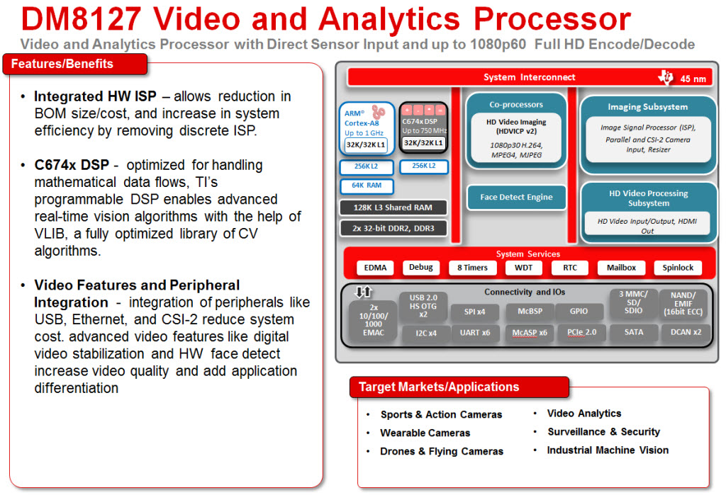
TMS320DM8127达芬奇数字媒体处理器是高度集成的可编程平台,利用该技术满足以下应用的处理需求,仅举几例:IP网络摄像机工业自动化网络摄像机立体摄像机视频监控高清视频会议汽车黑匣子家庭音频和视频设备

该设备使原始设备制造商(OEM)和原始设计制造商(ODM)能够快速推向市场强大的操作系统支持,丰富的用户界面和高处理性能,通过完全集成的混合处理器解决方案的最大灵活性。该器件还将可编程视频和音频处理与高度集成的外设集相结合。

可编程性由具有Neon扩展,TI C674x VLIW浮点DSP内核和高电平的ARM Cortex-A8 RISC CPU提供。定义视频和成像协处理器。 ARM允许开发人员将控制功能与DSP和协处理器上编程的A /V算法分开,从而降低系统软件的复杂性。具有Neon浮点扩展的ARM Cortex-A8 32位RISC内核包括:32KB指令缓存; 32KB的数据缓存; 256KB的L2 Cache; 48KB的Boot ROM;和64KB的RAM。

丰富的外设集可以控制外部外围设备并与外部处理器通信。有关每个外围设备的详细信息,请参阅本文档中的相关章节以及相关的外围设备参考指南。外设集包括:高清视频处理子系统双端口千兆以太网MAC(10/100/1000 Mbps)[以太网交换机],带有MII /RMII /GMII /RGMII和支持IEEE 1588时间戳,AVB和工业以太网协议的MDIO接口2 USB端口,集成2.0 PHY PCIe x1 GEN2兼容接口两个10串行器McASP音频串行端口(带DIT模式)四个四串行器McASP音频串行端口(带DIT模式)一个McBSP多通道缓冲串行端口六个UART,支持IrDA和CIR四个SPI串行接口三个MMC /SD /SDIO串行接口四个 2 C主从接口并行摄像机接口(CAM)多达128个通用I /O(GPIO)八个32位通用定时器系统看门狗定时器双DDR2和DDR3 SDRAM接口灵活的8位或16位异步存储器接口两个控制器局域网(DCAN)模块Spin LockMailbox

TMS320DM8127达芬奇数字媒体处理器还包括一个高清视频和想象g协处理器2(HDVICP2)可以从DSP内核卸载许多视频和图像处理任务,为常见的视频和成像算法提供更多的DSP MIPS。此外,TMS320DM8127达芬奇数字媒体处理器还为ARM和DSP提供了一整套开发工具,包括C编译器,简化编程和调度的DSP汇编优化器,以及用于查看源代码执行情况的Microsoft®Windows™调试器界面。

C674x DSP内核是TMS320C6000 DSP平台中的高性能浮点DSP生成器,与上一代C64x定点和C67x浮点DSP生成代码兼容。 C674x浮点DSP处理器使用32KB的L1程序存储器和EDC以及32KB的L1数据存储器。最多32KB的L1P可配置为程序缓存。剩余内存是不可缓存的无等待状态程序内存。最多可将32KB的L1D配置为数据高速缓存。剩余内存是不可缓存的无等待状态数据内存。 DSP具有256KB带有ECC的L2 RAM,可以定义为SRAM,L2高速缓存或两者的组合。所有C674x L3和片外

特性

  • High-Performance DaVinci Video Processors
    • Up to 1-GHz ARM® Cortex®-A8 RISC Core
    • Up to 750-MHz C674x VLIW DSP
    • Up to 6000 MIPS and 4500 MFLOPS
    • Fully Software-Compatible with C67x+, C64x+
  • ARM Cortex-A8 Core
    • ARMv7 Architecture
      • In-Order, Dual-Issue, Superscalar Processor Core
      • Neon™ Multimedia Architecture
      • Supports Integer and Floating Point
      • Jazelle® RCT Execution Environment
  • ARM Cortex-A8 Memory Architecture
    • 32KB of Instruction and Data Caches
    • 256KB of L2 Cache
    • 64KB of RAM, 48KB of Boot ROM
  • TMS320C674x Floating-Point VLIW DSP
    • 64 General-Purpose Registers (32-Bit)
    • Six ALU (32-/40-Bit) Functional Units
      • Supports 32-Bit Integer, SP (IEEE Single Precision/32-Bit) and DP (IEEE Double Precision/64-Bit) Floating Point
      • Supports up to Four SP Adds Per Clock and Four DP Adds Every Two Clocks
      • Supports up to Two Floating-Point (SP or DP) Approximate Reciprocal or Square Root Operations Per Cycle
    • Two Multiply Functional Units
      • Mixed-Precision IEEE Floating-Point Multiply Supported up to:
        • 2 SP x SP → SP Per Clock
        • 2 SP x SP → DP Every Two Clocks
        • 2 SP x DP → DP Every Three Clocks
        • 2 DP x DP → DP Every Four Clocks
      • Fixed-Point Multiply Supports Two 32 x 32 Multiplies, Four 16 x 16-Bit Multiplies Including Complex Multiplies, or Eight 8 x 8-Bit Multiplies per Clock Cycle
  • 128KB of On-Chip Memory Controller (OCMC) RAM
  • Imaging Subsystem (ISS)
    • Camera Sensor Connection
      • Parallel Connection for Raw (up to 16-Bit) and BT.656 or BT.1120 (8- and 16-Bit)
      • CSI2 Serial Connection
    • Image Sensor Interface (ISIF) for Handling Image and Video Data From the Camera Sensor
    • Image Pipe Interface (IPIPEIF) for Image and Video Data Connection Between Camera Sensor, ISIF, IPIPE, and DRAM
    • Image Pipe (IPIPE) for Real-Time Image and Video Processing
    • Resizer
      • Resizing Image and Video From 1/16x to 8x
      • Generating Two Different Resizing Outputs Concurrently
    • Hardware 3A Engine (H3A) for Generating Key Statistics for 3A (AE, AWB, and AF) Control
  • Face Detect Engine (FD)
    • Hardware Face Detection for up to 35 Faces at OPP100
  • Programmable High-Definition Video Image Coprocessing (HDVICP v2) Engine
    • Encode, Decode, Transcode Operations
    • H.264, MPEG-2, VC-1, MPEG-4, SP/ASP, JPEG/MJPEG
  • Media Controller
    • Controls the HDVPSS and ISS
  • Endianness
    • ARM and DSP Instructions/Data – Little Endian
  • HD Video Processing Subsystem (HDVPSS)
    • One 165-MHz HD Video Capture Input
      • One 16- or 24-Bit Input, Splittable into Dual 8-Bit SD Capture Ports
    • Two 165-MHz HD Video Display Outputs
      • One 16-, 24-, or 30-Bit Output and One 16- or 24-Bit Output
    • Composite or S-Video Analog Output
    • Macrovision® Support Available
    • Digital HDMI 1.3 Transmitter With Integrated PHY
    • Advanced Video Processing Features Such as Scan, Format, Rate Conversion
    • Three Graphics Layers and Compositors
  • Dual 32-Bit DDR2/DDR3 SDRAM Interfaces
    • Supports up to DDR2-800 and DDR3-1066
    • Up to Eight x 8 Devices Total 2GB of Total Address Space
    • Dynamic Memory Manager (DMM)
      • Programmable Multi-Zone Memory Mapping and Interleaving
      • Enables Efficient 2D Block Accesses
      • Supports Tiled Objects in 0°, 90°, 180°, or 270° Orientation and Mirroring
      • Optimizes Interlaced Accesses
  • General-Purpose Memory Controller (GPMC)
    • 8- or 16-Bit Multiplexed Address and Data Bus
    • 512MB of Address Space Divided Among up to 8 Chip Selects
    • Glueless Interface to NOR Flash, NAND Flash (BCH/Hamming Error Code Detection), SRAM and Pseudo-SRAM
    • Error Locator Module (ELM) Outside of GPMC to Provide Up to 16-Bit or 512-Byte Hardware ECC for NAND
    • Flexible Asynchronous Protocol Control for Interface to FPGA, CPLD, ASICs, and so Forth
  • Enhanced Direct Memory Access (EDMA) Controller
    • Four Transfer Controllers
    • 64 Independent DMA Channels and 8 Independent QDMA Channels
  • Dual Port Ethernet (10/100/1000 Mbps) With Optional Switch
    • IEEE 802.3 Compliant (3.3-V I/O Only)
    • MII/RMII/GMII/RGMII Media Independent Interfaces
    • Management Data I/O (MDIO) Module
    • Reset Isolation
    • IEEE 1588 Time-Stamping, AVB, and Industrial Ethernet Protocols
  • Dual USB 2.0 Ports With Integrated PHYs
    • USB2.0 High- and Full-Speed Clients
    • USB2.0 High-, Full-, and Low-Speed Hosts, or OTG
    • Supports End Points 0–15
  • One PCI Express 2.0 Port With Integrated PHY
    • Single Port With One Lane at 5.0 GT/s
    • Configurable as Root Complex or Endpoint
  • Eight 32-Bit General-Purpose Timers (Timer1–8)
  • One System Watchdog Timer (WDT0)
  • Six Configurable UART/IrDA/CIR Modules
    • UART0 With Modem Control Signals
    • Supports up to 3.6864 Mbps UART0/1/2
    • Supports up to 12 Mbps UART3/4/5
    • SIR, MIR, FIR (4.0 MBAUD), and CIR
  • Four Serial Peripheral Interfaces (SPIs) (up to
    48 MHz)
    • Each With Four Chip Selects
  • Three MMC/SD/SDIO Serial Interfaces (up to
    48 MHz)
    • Three Supporting up to 1-, 4-, or 8-Bit Modes
  • Four Inter-Integrated Circuit (I2C Bus) Ports
  • Six Multichannel Audio Serial Ports (McASPs)
    • Dual Ten Serializer Transmit and Receive Ports
    • Quad Four Serializer Transmit and Receive Ports
    • DIT-Capable For S/PDIF (All Ports)
  • Multichannel Buffered Serial Port (McBSP)
    • Transmit and Receive Clocks up to 48 MHz
    • Two Clock Zones and Two Serial Data Pins
    • Supports TDM, I2S, and Similar Formats
  • Real-Time Clock (RTC)
    • One-Time or Periodic Interrupt Generation
  • Up to 128 General-Purpose I/O (GPIO) Pins
  • One Spin Lock Module with up to 128 Hardware Semaphores
  • One Mailbox Module with 12 Mailboxes
  • On-Chip ARM ROM Bootloader (RBL)
  • Power, Reset, and Clock Management
    • Multiple Independent Core Power Domains
    • Multiple Independent Core Voltage Domains
    • Support for Three Operating Points (OPP100, OPP120, OPP166) per Voltage Domain
    • Clock Enable and Disable Control for Subsystems and Peripherals
  • 32KB of Embedded Trace Buffer (ETB) and
    5-Pin Trace Interface for Debug
  • IEEE 1149.1 (JTAG) Compatible
  • 684-Pin Pb-Free BGA Package (CYE Suffix), 0.8-mm Ball Pitch With Via Channel Technology to Reduce PCB Cost
  • 45-nm CMOS Technology
  •  

参数 与其它产品相比 数字视频处理器

 
Applications
Operating Systems
Arm CPU
Arm MHz (Max.)
DSP
DSP MHz
Video Acceleration
Video Resolution/Frame Rate
Video Port (Configurable)
USB
PCI/PCIe
EMAC
DRAM
SPI
I2C
UART (SCI)
On-Chip L2 Cache/RAM
Operating Temperature Range (C)
Pin/Package
TMS320DM8127
Machine Vision
Industrial Cameras
Portable Cameras
Video Surveillance IP Cameras    
0    
1 ARM Cortex-A8    
1000    
1 C674x    
750    
1 HDVICP    
1080P
60FPS or less    
2 Output
1 Input
2 SD DACs
1 HDMI TX    
2 USB2.0 w/phy    
PCIe x1 GEN2    
10/100/1000 2-port    
LPDDR
DDR2
DDR3    
4    
4    
6    
256 KB    
-40 to 90
0 to 90    
684FCBGA    

方框图 (3)

技术文档

数据手册(1)
元器件购买 TMS320DM8127 相关库存