| Number of channels (#) | 1 |
| Total supply voltage (Max) (+5V=5, +/-5V=10) | 5.5 |
| Total supply voltage (Min) (+5V=5, +/-5V=10) | 4.5 |
| Rail-to-rail | In, Out |
| GBW (Typ) (MHz) | 1 |
| Slew rate (Typ) (V/us) | 1.4 |
| Vos (offset voltage @ 25 C) (Max) (mV) | 100 |
| Iq per channel (Typ) (mA) | 2 |
| Vn at 1 kHz (Typ) (nV/rtHz) | 12 |
| Rating | Catalog |
| Operating temperature range (C) | -40 to 125 |
| Offset drift (Typ) (uV/C) | 1.5 |
| CMRR (Typ) (dB) | 80 |
| Output current (Typ) (mA) | 55 |
- Typical Values, TA = 25°C, V+=5V, V-=0V.
- Gain Bandwidth 1 MHz
- Input Voltage Range (G= 0.096 V/V) -15V to +15V
- Core Op-Amp Input Offset Voltage 100 μV (Max)
- Supply Current 2 mA (Max)
- Gain (Attenuation Mode) 0.096 V/V, 0.192 V/V0.384 V/V, 0.768 V/V
- Gain (Amplification Mode) 1 V/V, 2 V/V
- Gain Error 0.035% (Max)
- Core Op-Amp PSRR 90 dB (Min)
- CMRR 80 dB (min)
- Adjustable Output Common Mode 1V to 4V
- Temperature Range ?40 to 125°C
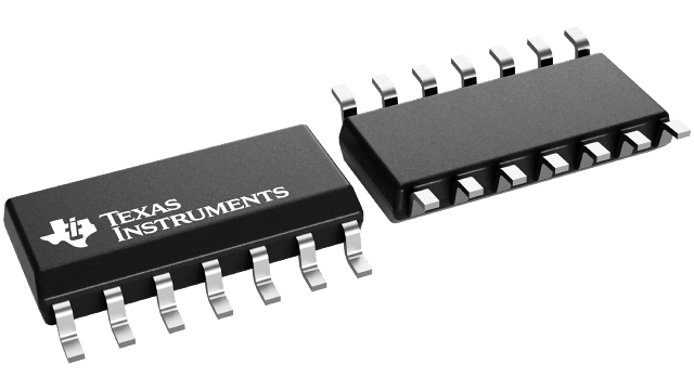
- Package 14-Pin SOIC
All trademarks are the property of their respective owners.
The LMP7312 is a digitally programmable variable gain amplifier/attenuator. Its wide input voltage range and superior precision make it a prime choice for applications requiring high accuracy such as data acquisition systems for IO modules in programmable logic control (PLC). The LMP7312 provides a differential output to maximize dynamic range and signal to noise ratio, thereby reducing the overall system error. It can also be configured to handle single ended input data converters by means of the VOCM pin (see for details). The inputs of LMP7312 can be configured in attenuation mode to handle large input signals of up to +/- 15V, as well as in amplification mode to handle current loops of 0-20mA and 4-20mA.The LMP7312 is equipped with a null switch to evaluate the offset of the internal amplifier. A ensured 0.035% maximum gain error (for all gains) and a maximum gain drift of 5ppm over the extended industrial temperature range (-40° to 125°C) make the LMP7312 very attractive for high precision systems even under harsh conditions. A low input offset voltage of 100μV and low voltage noise of 3μVpp give the LMP7312 a superior performance. The LMP7312 is fully specified from -40° to 125°C and is available in SOIC-14 package.


