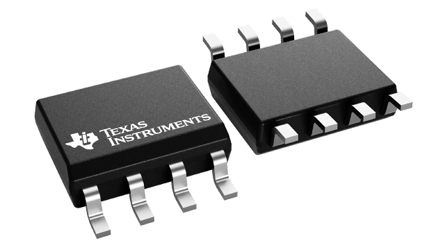
| Number of channels (#) | 2 |
| Total supply voltage (Max) (+5V=5, +/-5V=10) | 32 |
| Total supply voltage (Min) (+5V=5, +/-5V=10) | 3 |
| Rail-to-rail | In to V- |
| GBW (Typ) (MHz) | 0.7 |
| Slew rate (Typ) (V/us) | 0.3 |
| Vos (offset voltage @ 25 C) (Max) (mV) | 3 |
| Iq per channel (Typ) (mA) | 0.35 |
| Vn at 1 kHz (Typ) (nV/rtHz) | 40 |
| Rating | HiRel Enhanced Product |
| Operating temperature range (C) | -55 to 125 |
| Offset drift (Typ) (uV/C) | 7 |
| Input bias current (Max) (pA) | 15000 |
| CMRR (Typ) (dB) | 80 |
| Output current (Typ) (mA) | 30 |
| Architecture | Bipolar |
- Controlled Baseline
- One Assembly/One Test Site, One Fabrication Site
- Extended Temperature Performance of -55°C to 125°C
- Enhanced Diminishing Manufacturing Sources (DMS) Support
- Enhanced Product-Change Notification
- Qualification Pedigree(1)
- Wide Supply Range:
- Single Supply . . . 3 V to 30 V
- Dual Supplies . . .±1.5 V to ±15 V
- Low Supply-Current Drain, Independent of Supply Voltage . . . 0.7 mA Typ
- Common-Mode Input Voltage Range Includes Ground, Allowing Direct Sensing Near Ground
- Low Input Bias and Offset Parameters:
- Input Offset Voltage . . . 2 mV Typ
- Input Offset Current . . . 2 nA Typ
- Input Bias Current . . . 15 nA Typ
- Differential Input Voltage Range Equal to Maximum-Rated Supply Voltage . . . 32 V
- Open-Loop Differential Voltage Amplification . . . 100 V/mV Typ
- Internal Frequency Compensation
(1) Component qualification in accordance with JEDEC and industry standards to ensure reliable operation over an extended temperature range. This includes, but is not limited to, Highly Accelerated Stress Test (HAST) or biased 85/85, temperature cycle, autoclave or unbiased HAST, electromigration, bond intermetallic life, and mold compound life. Such qualification testing should not be viewed as justifying use of this component beyond specified performance and environmental limits.
The LM258A consists of two independent, high-gain, frequency-compensated operational amplifiers designed to operate from a single supply over a wide range of voltages. Operation from split supplies also is possible if the difference between the two supplies is 3 V to 30 V, and VCC is at least 1.5 V more positive than the input common-mode voltage. The low supply-current drain is independent of the magnitude of the supply voltage.
Applications include transducer amplifiers, dc amplification blocks, and all the conventional operational amplifier circuits that now can be implemented more easily in single-supply-voltage systems. For example, this device can be operated directly from the standard 5-V supply used in digital systems and easily can provide the required interface electronics without additional ±5-V supplies.


