| Architecture | Voltage FB |
| Number of channels (#) | 4 |
| Total supply voltage (Min) (+5V=5, +/-5V=10) | 5 |
| Total supply voltage (Max) (+5V=5, +/-5V=10) | 12 |
| GBW (Typ) (MHz) | 250 |
| BW @ Acl (MHz) | 650 |
| Acl, min spec gain (V/V) | 1 |
| Slew rate (Typ) (V/us) | 240 |
| Vn at flatband (Typ) (nV/rtHz) | 2.5 |
| Vn at 1 kHz (Typ) (nV/rtHz) | 2.5 |
| Iq per channel (Typ) (mA) | 5.6 |
| Vos (offset voltage @ 25 C) (Max) (mV) | 0.8 |
| Rail-to-rail | No |
| Rating | Catalog |
| Operating temperature range (C) | -40 to 85 |
| CMRR (Typ) (dB) | 85 |
| Input bias current (Max) (pA) | 20000000 |
| Offset drift (Typ) (uV/C) | 4 |
| Output current (Typ) (mA) | 85 |
| 2nd harmonic (dBc) | 84 |
| 3rd harmonic (dBc) | 92 |
| Frequency of harmonic distortion measurement (MHz) | 1 |
- HIGH BANDWIDTH: 220MHz (G = +2)
- HIGH OUTPUT CURRENT: ±85mA
- LOW INPUT NOISE: 2.5nV/
 Hz
Hz - LOW SUPPLY CURRENT: 5.7mA/ch
- FLEXIBLE SUPPLY VOLTAGE:
±2V to ±6.3V Dual Supply
+4V to +12.6V Single Supply - EXCELLENT DC ACCURACY:
- Maximum 25°C Input Offset Voltage = 0.8mV
- Maximum 25°C Input Offset Current = 500nA
- APPLICATIONS
- LOW–COST VIDEO LINE DRIVERS
- ADC PREAMPS
- ACTIVE FILTERS
- LOW–NOISE INTEGRATORS
- PORTABLE TEST EQUIPMENT
- OPTICAL CHANNEL AMPLIFIERS
- LOW–POWER, BASEBAND AMPLIFIERS
- CCD IMAGING CHANNEL AMPLIFIERS
- OPA4650 UPGRADE
All trademarks are the property of their respective owners.
The OPA4820 provides a wideband, unity-gain stable, voltage-feedback amplifier with a very low input noise voltage and high output current using a low 5.7mA/ch supply current. At unity-gain, the OPA4820 gives > 600MHz bandwidth with < 1 dB peaking. The OPA4820 complements this high-speed operation with excellent DC precision in a low-power device. A worst-case input offset voltage of ±0.8mV and an offset current of ±500nA give excellent absolute DC precision for pulse amplifier applications.
Minimal input and output voltage swing headroom allow the OPA4820 to operate on a single +5V supply with > 2VPP output swing. While not a rail-to-rail (RR) output, this swing will support most emerging analog-to-digital converter (ADC) input ranges with lower power and noise than typical RR output op amps.
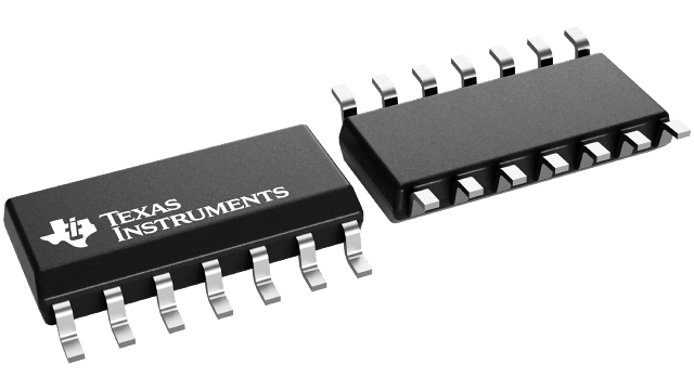
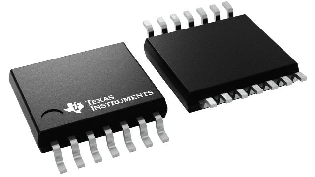
Exceptionally low dG/dP (0.01%/0.03°) supports low-cost composite video line driver applications. Existing designs can use the industry-standard quad pinout SO-14 package while emerging high-density portable applications can use the TSSOP-14.


