| Number of ADC channels | 1 |
| Number of DAC channels (#) | 1 |
| Digital audio interface | DSP |
| Analog inputs | 2 |
| Sampling rate (Max) (kHz) | 22.05 |
| Rating | Catalog |
| ADC SNR (Typ) (dB) | 87 |
| DAC SNR (Typ) (dB) | 90 |
| | |
- C54xx software driver available
- 16-bit oversampling sigma-delta A/D converter
- 16-bit oversampling sigma-delta D/A converter
- Maximum output conversion rate:
- 22 ksps with on-chip FIR filter
- 88 ksps with FIR bypassed
- Voiceband bandwidth in FIR-bypassed mode and final sampling rate at 8 ksps
- 90-dB SNR/ADC and 87-dB SNR/DAC with DSPs FIR (FIR bypassed at 88 ksps/5 V)
- 87-dB SNR/ADC and 85-dB SNR/DAC with DSPs FIR (FIR bypassed at 88 ksps/3.3 V)
- On-chip FIR produced 84-dB SNR for ADC and 85-dB SNR for DAC over 11-kHz BW
- Built-in functions including PGA, antialiasing analog filter, and operational amplifiers for general-purpose interface (such as MIC interface and hybrid interface)
- Glueless serial port interface to DSPs (TI TMS320Cxx, SPI, or standard DSPs)
- Automatic cascading detection (ACD) makes cascade programming simple and allows up to 8 devices to be connected in cascade.
- On-fly reconfiguration modes include secondary-communication mode and direct-configuration mode (host interface).
- Continuous data-transfer mode for use with autobuffering (ABU) to reduce DSP interrupt service overhead
- Event-monitor mode provides external-event control, such as RING/OFF-HOOK detection
- Programmable ADC and DAC conversion rate
- Programmable input and output gain control
- Separate software control for ADC and DAC power-down
- Analog (3-V to 5.5-V) supply operation
- Digital (3-V to 5.5-V) supply operation
- Power dissipation (PD) of 39 mWrms typical for 8-ksps at 3.3 V
- Hardware power-down mode to 0.5 mW
- Internal and external reference voltage (Vref)
- Differential and single-ended analog input/output
- 2s-complement data format
- Test mode, which includes digital loopback and analog loopback
- 600-ohm output driver
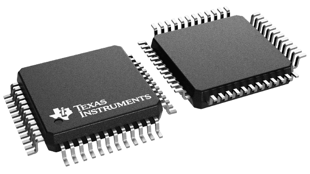
The TLV320AIC10 provides high resolution signal conversion from digital-to-analog (D/A) and from analog-to-digital (A/D) using oversampling sigma-delta technology. It allows 2-to-1 MUX inputs with built-in antialiasing filter and amplification for general-purpose applications such as telephone hybrid interface, electret microphone preamp, etc. Both IN and AUX inputs accept normal analog signals. This device consists of a pair of 16-bit synchronous serial conversion paths (one for each direction), and includes an interpolation filter before the DAC and a decimation filter after the ADC. The FIR filters can be bypassed to offer flexibility and power savings. Other overhead functions provide on-chip include timing (programmable sample rate, continuous data transfer, and FIR bypass) and control (programmable-gain amplifier, communication protocol, etc.). The sigma-delta architecture produces high-resolution analog-to-digital and digital-to-analog conversion at low system cost.
The TLV320AIC10 design enhances communication with the DSP. The continuous data transfer mode fully supports TI?s DSP autobuffering (ABU) to reduce DSP interrupt service overhead. The automatic cascading detection (ACD) makes cascade programming simple and supports a cascade operation of one master and up to seven slaves. The direct-configuration mode for host interface uses a single-wire serial port to directly program internal registers without interference from the data conversion serial port, or without resetting the entire device. The event monitor mode allows the DSP to monitor external events like phone off-hook ring detection.
In the lower-power mode, the TLV320AIC10 converts data at a sampling rate of 8 KSPS consuming only 39 mW.
The programmable functions of this device are configured through a serial interface that can be gluelessly interfaced to any DSP that accepts 4-wire serial communications, such as the TMS320Cxx. The options include software reset, device power-down, separate control for ADC and DAC turnoff, communications protocol, signal-sampling rate, gain control, and system-test modes, as outlined in Appendix A.
The TLV320AIC10 is particularly suitable for a variety of applications in hands-free car kits, VOIP, cable modem, speech, and the telephony area including low-bit rate, high-quality compression, speech enhancement, recognition, and synthesis. Its low-group delay characteristic makes it suitable for single or multichannel active-control applications.
The TLV320AIC10 is characterized for commercial operation from 0°C to 70°C, and industrial operation from ?40°C to 85°C.


