| Number of ADC channels | 1 |
| Number of DAC channels (#) | 1 |
| Analog inputs | 2 |
| Sampling rate (Max) (kHz) | 22.05 |
| Rating | Military |
| ADC SNR (Typ) (dB) | 0 |
| DAC SNR (Typ) (dB) | 0 |
| | |
- General-purpose analog interface circuit for V.34+ modem and business audio applications
- 16-bit oversampling sigma-delta ADC and DAC
- Serial port interface
- Typical 89-dB SNR (signal-to-noise ratio) for ADC and DAC
- Typical 90-dB THD (signal to total harmonic distortion) for ADC and DAC
- Typical 88-dB dynamic range
- Test mode that includes a digital loopback test and analog loopback test
- Programmable A/D and D/A conversion rate
- Programmable input and output gain control
- Maximum conversion rate: 22.05 kHz
- Single 5-V power supply voltage or 5-V analog and 3-V digital power supply voltage
- Power dissipation (PD) of 120 mW rms typical in the operating mode
- Hardware power-down mode to 7.5 mW
- Internal reference voltage (Vref)
- Differential architecture throughout device
- TLC320AD50C/I can support up to three slave devices; TLC320AD52C can support one slave
- 2s complement data format
- ALTDATA terminal provides data monitoring
- Monitor amplifier to monitor input signals
- On-chip phase locked loop (PLL)
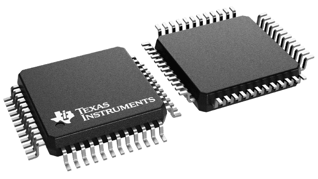
The TLC320AD50C, TLC320AD50I, and TLC320AD52C provide high-resolution signal conversion from digital-to-analog (D/A) and from analog-to-digital (A/D) using oversampling sigma-delta technology. This device consists of a pair of 16-bit synchronous serial conversion paths (one for each direction) and includes an interpolation filter before the DAC and a decimation filter after the ADC. Other overhead functions on the chip include timing (sample rate, FSD delay) and control (programmable gain amplifier, PLL, communication protocol, etc.). The sigma-delta architecture produces high resolution A/D and D/A conversion at a low system cost.
Programmable functions of this device can be selected through the serial interface. Options include reset, power down, communications protocol, signal sampling rate, gain control, and system test modes (see section 6). The TLC320AD50C and TLC320AD52C are characterized for operation from 0°C to 70°C, and the TLC320AD50I is characterized for operation from \x9640°C to 85°C.


