| Function | Spread-spectrum clock generator |
| Number of outputs | 1 |
| Output frequency (Max) (MHz) | 108 |
| Core supply voltage (V) | 3.3 |
| Output supply voltage (V) | 3.3 |
| Input type | XTAL |
| Output type | LVCMOS |
| Operating temperature range (C) | -40 to 85 |
| Features | Multiplier or divider, Spread-spectrum clocking (SSC), Pin programmable |
| Rating | Catalog |
- Part of a Family of Easy to use Clock Generator Devices With Optional SSC
- Crystal Oscillator With Integrated Crystal Capacitors, Selectable Output Frequency and Selectable SSC
- SSC Controllable via 2 External Pins
- ±0%, ±0.5%, ±1%, ±2% Center Spread
- Frequency Multiplication Selectable Between x1 or x4 With one External Control Pin
- Single 3.3V Device Power Supply
- Wide Temperature Range -40°C to 85°C
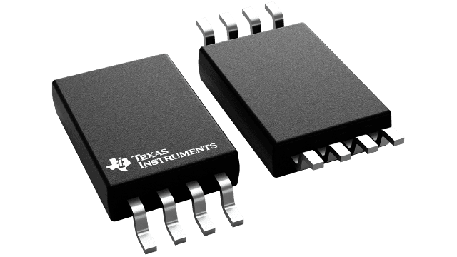
- Low space Consumption by 8 pin TSSOP Package
- APPLICATIONS
- Consumer and Industrial Applications requiring Crystal Oscillator with the possibility of EMI reduction through Spread Spectrum Clocking
The CDCS502 is a spread spectrum capable, fundamental mode crystal oscillator with selectable frequency multiplication.
It features an advanced gain controlled fundamental mode crystal oscillator stage with a built-in load capacitance of 10pF. This oscillator stage accepts crystals from 8MHz to 32MHz with an ESR of up to 180Ω. The stage can be used with crystals with power dissipation of 50μW and up.
The input signal is processed by a PLL, whose output frequency is either equal to the input frequency or multiplied by the factor of 4.
The PLL is also able to spread the clock signal by ±0%, ±0.5%, ±1% or ±2% centered around the output clock frequency with an triangular modulation.
By this, the device can generate output frequencies between 8MHz and 108MHz with or without SSC from a fundamental mode crystal.
In x1 Mode with an SSC amount of 0%, the device works as a standard crystal oscillator and does not make use of the built in PLL.
The CDCS502 operates in 3.3V environment.
It is characterized for operation from -40°C to 85°C. It is offered in an 8 Pin TSSOP package.


