730kSPS、12 位、6 通道、同步采样 ADC
| Resolution (Bits) | 12 |
| Number of input channels | 6 |
| Sample rate (Max) (kSPS) | 730 |
| Interface type | Parallel, Byte-Wide, SPI |
| Architecture | SAR |
| Input type | Single-Ended |
| Multi-channel configuration | Simultaneous Sampling |
| Rating | Catalog |
| Reference mode | Ext, Int |
| Input range (Max) (V) | 12 |
| Input range (Min) (V) | -12 |
| Features | Daisy-Chainable, Oscillator |
| Operating temperature range (C) | -40 to 125 |
| Power consumption (Typ) (mW) | 335 |
| Analog voltage AVDD (Min) (V) | 4.5 |
| SNR (dB) | 73.9 |
| Analog voltage AVDD (Max) (V) | 5.5 |
| INL (Max) (+/-LSB) | 0.75 |
| Digital supply (Min) (V) | 2.7 |
| Digital supply (Max) (V) | 5.5 |
- Family of 16-, 14-, 12-Bit, Pin- and
Software-Compatible ADCs - Six SAR ADCs Grouped in Three Pairs
- Maximum Data Rate Per Channel with Internal
Conversion Clock and Reference:
ADS8556: 630 kSPS (PAR) or 450 kSPS (SER)
ADS8557: 670 kSPS (PAR) or 470 kSPS (SER)
ADS8558: 730 kSPS (PAR) or 500 kSPS (SER) - Maximum Data Rate with External Conversion
Clock and Reference:
800 kSPS (PAR) or 530 kSPS (SER) - Pin-Selectable or Programmable Input Voltage
Ranges: Up to ±12 V - Excellent Signal-to-Noise Performance:
ADS8556: 91.5 dB, ADS8667: 85 dB,
ADS8668: 73.9 dB - Programmable and Buffered Internal Reference:
0.5 V to 2.5 V and 0.5 V to 3.0 V - Comprehensive Power-Down Modes:
- Deep Power-Down (Standby Mode)
- Partial Power-Down
- Auto-Nap Power-Down
- Selectable Parallel or Serial Interface
- Operating Temperature Range: –40°C to 125°C
The ADS855x contains six low-power, 16-, 14-, or 12-bit, successive approximation register (SAR) based analog-to-digital converters (ADCs) with true bipolar inputs. Each channel contains a sample-and-hold circuit that allows simultaneous high-speed multi-channel signal acquisition.
The ADS855x supports data rates of up to 730 kSPS in parallel interface mode or up to 500 kSPS if the serial interface is used. The bus width of the parallel interface can be set to eight or 16 bits. In serial mode, up to three output channels can be activated.
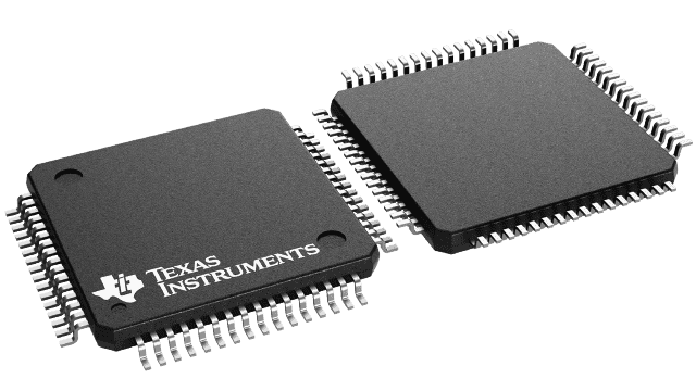
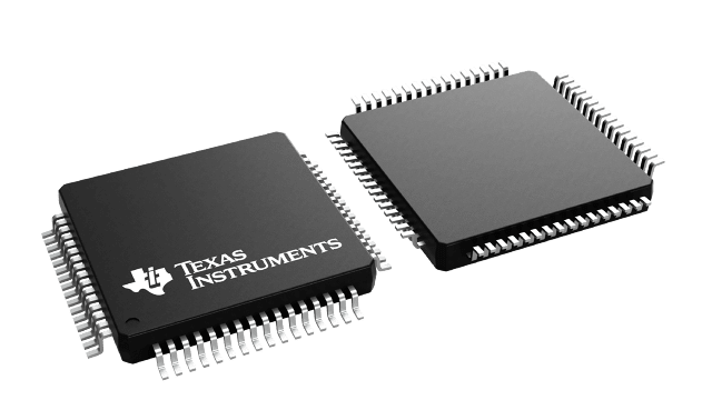
The ADS855x is specified over the full industrial temperature range of ?40°C to 125°C and is available in an LQFP-64 package.


