| Resolution (Bits) | 24 |
| Number of DAC channels (#) | 1 |
| Interface type | Bitstream |
| Output type | Unbuffered Current |
| Settling time (μs) | 100 |
| Reference type | Ext |
| Architecture | Current-Steering |
| Rating | Catalog |
| Output range (Max) (mA/V) | 2.5 |
| Output range (Min) (mA/V) | 0.039 |
| Operating temperature range (C) | -40 to 85 |
- Outstanding Performance:
- THD: –125dB
- SNR: 120dB (413Hz BW, Gain = 1/1)
- Gain Error: 0.1%
- Pin Operation: No Registers to Program
- Gain: 1/1 to 1/64
- SYNC Input for Phase Control
- Power-Down Mode
- Low Power: 18mW
- Analog Supply: +5V or ±2.5V
- Digital Supply: 1.8V to 3.3V
- Small 16-Pin TSSOP Package
- Temperature Range: –40°C to +85°C
- APPLICATIONS
- Energy Exploration Equipment
- Seismic Monitoring Systems
All other trademarks are the property of their respective owners
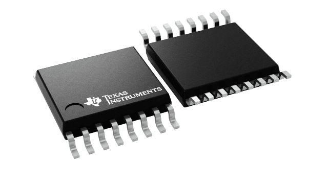
The DAC1280 is a very low distortion digital-to-analog converter (DAC) suited for performance testing of seismic equipment. The DAC1280 provides a high-accuracy output signal from a bitstream input. The device achieves very high linearity in a small package while dissipating only 18mW. Together with the high-performance ADS1281 and ADS1282 analog-to-digital converters (ADCs), these devices create a test and measurement system that meets the exacting demands of energy exploration and seismic monitoring equipment.
The DAC1280 is designed to match the system components (power supply, clock and reference voltage) of the companion ADCs, the ADS1281 and ADS1282. The input to the DAC1280 is a 1s density modulated bitstream. The DAC1280 output is a differential current intended for use with an active I/V converter. The I/V converter provides a voltage output suitable for performance testing of sensors and ADCs.
Three gain control pins set the output range in 6dB steps from 0dB to –36db (±2.5V to ±0.039V differential). The attenuation ranges match the gains of the ADS1282 for testing at all gains. The DAC uses a reference voltage and bias resistor to set the full-scale output. The resistor can be adjusted to fine-trim the DAC full-scale.
The SYNC pin aligns the input data sampling to the CLK phase. A power-down pin shuts down the device when not in use. The DAC1280 is available in a small, 16-pin TSSOP package and is fully specified for operation over –40°C to +85°C temperature range with a maximum operating temperature of +125°C.


