| Resolution (Bits) | 12 |
| Number of DAC channels (#) | 4 |
| Interface type | SPI |
| Output type | Buffered Voltage |
| Settling time (μs) | 6 |
| Features | On-chip Offset and Gain Calibration, SDO |
| Reference type | Ext |
| Architecture | R-2R |
| Rating | Catalog |
| Output range (Max) (mA/V) | 16.5 |
| Output range (Min) (mA/V) | -16.5 |
| Operating temperature range (C) | -40 to 105 |
- Bipolar Output: Up to ±16V
- Unipolar Output: 0V to +20V
- 12-Bit Monotonic
- Relative Accuracy: 1 LSB Max
- Low Zero and Gain Errors
- Before User Calibration: 0.5 LSB
- After User Calibration:
0.0078 LSB Zero Error, 0.0625 LSB Gain Error
- Low Noise: 60nV/
 Hz
Hz - Settling Time: 6μs
- Configurable Gain: x2/x4
- Analog Output Monitor
- Power-Down Mode
- SPI: Up to 50MHz, 1.8V/3V/5V Logic
- Daisy-Chain Mode
- Operating Temperature: -40°C to +105°C
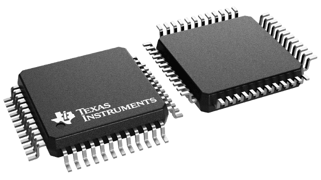
- Packages: QFN-40 (6x6mm), TQFP-48 (7x7mm)
- APPLICATIONS
- Automatic Test Equipment
- Instrumentation
- Industrial Process Control
- Communications
All trademarks are the property of their respective owners.
The DAC7716 is a high-accuracy, quad-channel, 12-bit digital-to-analog converter (DAC) that operates from supply voltages of ±5V to ±18V in bipolar output mode, and from ±5V to +24V/-12V in unipolar mode. With a 5V reference, the DAC7716 can be configured to output ±10V, ±5V, 0V to 20V, or 0V to 10V. The DAC7716 provides 12-bit monotonicity, excellent integral nonlinearity (INL) error of ±1 LSB, low glitch, and low noise over the operating temperature range of -40°C to +105°C. This device is trimmed in production for very low zero and gain errors. In addition, the DAC7716 implements a user-programmable system-level calibration function to achieve ±0.0078 LSB zero error and ±0.0625 LSB gain error.
The DAC7716 has integrated reference buffers and output buffers. It features a standard high-speed 1.8V, 3V, or 5V serial peripheral interface (SPI) that operates at clock rates of up to 50MHz to communicate with a DSP or microprocessor. The four DAC channels and the auxiliary registers are addressed with four address bits. The device features double-buffered interface logic for simultaneous updates of all DACs. An asynchronous load input (LDAC) transfers data from the input data register to the DAC latch, and the contents of the DAC latch set the output voltage. The asynchronous RST input sets the output of all four DACs to 0V. The VMON pin is an analog monitor output that multiplexes the individual DAC outputs or the AIN pin.
The DAC7716 is pin-compatible with the DAC8734 (16-bit) and the DAC8234 (14-bit).


