| Resolution (Bits) | 10 |
| Number of DAC channels (#) | 2 |
| Interface type | SPI |
| Output type | Buffered Voltage |
| Settling time (μs) | 6 |
| Features | Cost Optimized, Low Power, Small Size |
| Reference type | Ext |
| Architecture | String |
| Rating | Catalog |
| Output range (Max) (mA/V) | 5.5 |
| Output range (Min) (mA/V) | 0 |
| Operating temperature range (C) | -40 to 105 |
- Ensured Monotonicity
- Low Power Operation
- Rail-to-Rail Voltage Output
- Power-On Reset to 0 V
- Simultaneous Output Updating
- Wide Power Supply Range (2.7 V to 5.5 V)
- Industry’s Smallest Package
- Power Down Modes
- Key Specifications
- Resolution: 10 Bits
- INL: ±2 LSB (Maximum)
- DNL: +0.35 or –0.25 LSB (Maximum)
- Settling Time: 6 μs (Maximum)
- Zero Code Error: 15 mV (Maximum)
- Full-Scale Error: –0.75% FS (Maximum)
- Supply Power
- Normal: 0.6 mW at 3 V, 1.6 mW at 5 V
(Typical) - Power Down: 0.3 μW at 3 V, 0.8 μW at 5 V
(Typical)
- Normal: 0.6 mW at 3 V, 1.6 mW at 5 V
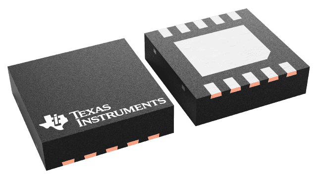
The DAC102S085 is a full-featured, general-purpose DUAL 10-bit voltage-output digital-to-analog converter (DAC) that can operate from a single 2.7-V to 5.5-V supply and consumes 0.6 mW at 3 V and 1.6 mW at 5 V. The DAC102S085 is packaged in 10-pin WSON and VSSOP packages. The 10-pin WSON package makes the DAC102S085 the smallest DUAL DAC in its class. The on-chip output amplifier allows rail-to-rail output swing and the three wire serial interface operates at clock rates up to 40 MHz over the entire supply voltage range. Competitive devices are limited to 25-MHz clock rates at supply voltages in the 2.7-V to 3.6-V range. The serial interface is compatible with standard SPI?, QSPI, MICROWIRE and DSP interfaces.
The reference for the DAC102S085 serves both channels and can vary in voltage between 1 V and VA, providing the widest possible output dynamic range. The DAC102S085 has a 16-bit input shift register that controls the outputs to be updated, the mode of operation, the power-down condition, and the binary input data. Both outputs can be updated simultaneously or individually depending on the setting of the two mode of operation bits.
A power-on reset circuit ensures that the DAC output powers up to zero volts and remains there until there is a valid write to the device. A power-down feature reduces power consumption to less than a microWatt with three different termination options.
The low power consumption and small packages of the DAC102S085 make it an excellent choice for use in battery-operated equipment.
The DAC102S085 is one of a family of pin compatible DACs, including the 8-bit DAC084S085 and the 12-bit DAC122S085. The DAC102S085 operates over the extended industrial temperature range of ?40°C to 105°C.


