| Resolution (Bits) | 16 |
| Number of DAC channels (#) | 1 |
| Interface type | Parallel |
| Output type | Buffered Voltage |
| Settling time (μs) | 10 |
| Features | Low Power, Reset to Mid-Scale |
| Reference type | Ext |
| Architecture | String |
| Rating | Catalog |
| Output range (Max) (mA/V) | 5.5 |
| Output range (Min) (mA/V) | 0 |
| Operating temperature range (C) | -40 to 85 |
- Micropower Operation: 250 uA at 5 V AVDD
- Power-On Reset to Min-Scale
- 16-Bit Monotonic
- Settling Time: 10 us to ±0.003% FSR
- 16-Bit Parallel Interface
- On-Chip Output Buffer Amplifier With Rail-to-Rail Operation
- Hardware Reset to Min-Scale or Mid-Scale
- Double-Buffered Architecture
- Asynchronous LDAC Control
- Data Readback Support
- 1.8 V Compatible Digital Interface:
- DVDD = 1.8 V–5.5 V
- Wide Analog Supply Range:
- AVDD = 2.7 V–5.5 V
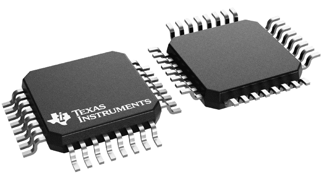
- 32-Lead 5 mm × 5 mm TQFP Package
- APPLICATIONS
- Process Control
- Data Acquisition Systems
- Closed-Loop Servo Control
- PC Peripherals
- Portable Instrumentation
The DAC8541 is a low-power, single channel, 16-bit, voltage output DAC. Its on-chip precision output amplifier allows rail-to-rail voltage swing to be achieved at the output. The DAC8541 utilizes a 16-bit parallel interface and features additional powerdown function pins as well as hardware-enabled, asynchronous DAC updating and reset capability.
The DAC8541 requires an external reference voltage to set the output range of the DAC. The device incorporates a power-on-reset circuit that ensures that the DAC output powers up at min-scale and remains there until a valid write takes place to the device. In addition, the DAC8541 contains a power-down feature, accessed via two hardware pins, that when enabled reduces the current consumption of the device to 200 nA at 5 V.
The low power consumption of this device in normal operation makes it ideally suited for use in portable battery operated equipment applications. The power consumption is 1.2 mW at AVDD = 5 V reducing to 1 uW in power-down mode.
The DAC8541 is available in a 32-lead TQFP package with an operating temperature range of ?40°C to 85°C.


