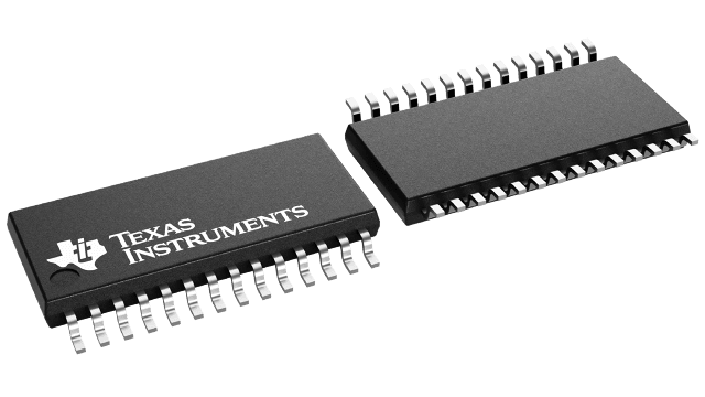
| Drivers per package | 5 |
| Receivers per package | 3 |
| Logic voltage (Min) (V) | 3.3 |
| Data rate (Max) (kbps) | 250 |
| Main supply voltage (Nom) (V) | 3.3, 5 |
| Features | Auto-Powerdown Plus |
| ESD HBM (kV) | 15 |
| Rating | Catalog |
| Operating temperature range (C) | -40 to 85, 0 to 70 |
| Vout (Typ) (V) | 5.4 |
- RS-232 Bus-Pin ESD Protection Exceeds
±15 kV Using Human-Body Model (HBM) - Meets or Exceeds the Requirements of TIA/EIA-232-F and ITU v.28 Standards
- Operates With 3-V to 5.5-V VCC Supply
- Operates up to 250 kbit/s
- Five Drivers and Three Receivers
- Low Standby Current . . . 1 μA Typical
- External Capacitors . . . 4 × 0.1 μF
- Accepts 5-V Logic Input With 3.3-V Supply
- Always-Active Noninverting Receiver Output (ROUT1B)
- Alternative High-Speed Pin-Compatible Device (1 Mbit/s)
- TRSF3238
- APPLICATIONS
- Battery-Powered Systems
- PDAs
- Notebooks
- Subnotebooks
- Laptops
- Palmtop PCs
- Hand-Held Equipment
- Modems
- Printers
The TRS3238 consists of five line drivers, three line receivers, and a dual charge-pump circuit with ±15-kV ESD (HBM) protection pin to pin (serial-port connection pins, including GND). The device meets the requirements of TIA/EIA-232-F and provides the electrical interface between notebook and subnotebook computer applications. The charge pump and four small external capacitors allow operation from a single 3-V to 5.5-V supply. In addition, the device includes an always-active noninverting output (ROUT1B), which allows applications using the ring indicator to transmit data while the device is powered down. The TRS3238 operates at data signaling rates up to 250 kbit/s and a maximum of 30-V/μs driver output slew rate.
Flexible control options for power management are featured when the serial port and driver inputs are inactive. The auto-powerdown plus feature functions when FORCEON is low and FORCEOFF is high. During this mode of operation, if the device does not sense valid signal transitions on all receiver and driver inputs for approximately 30 s, the built-in charge pump and drivers are powered down, reducing the supply current to 1 μA. By disconnecting the serial port or placing the peripheral drivers off, auto-powerdown plus occurs if there is no activity in the logic levels for the driver inputs. Auto-powerdown plus can be disabled when FORCEON and FORCEOFF are high. With auto-powerdown plus enabled, the device activates automatically when a valid signal is applied to any receiver or driver input. INVALID is high (valid data) if any receiver input voltage is greater than 2.7 V or less than -2.7 V, or has been between -0.3 V and 0.3 V for less than 30 μs. INVALID is low (invalid data) if all receiver input voltages are between -0.3 V and 0.3 V for more than 30 μs. Refer to Figure 5 for receiver input levels.


