| Technology Family | LVC |
| Supply voltage (Min) (V) | 1.65 |
| Supply voltage (Max) (V) | 3.6 |
| Number of channels (#) | 8 |
| IOL (Max) (mA) | 24 |
| ICC (Max) (uA) | 10 |
| IOH (Max) (mA) | -24 |
| Input type | Standard CMOS |
| Output type | 3-State |
| Features | Balanced outputs, Very high speed (tpd 5-10ns), Bus-hold |
| Rating | Catalog |
- Operate From 1.65 V to 3.6 V
- Inputs Accept Voltages to 5.5 V
- Max tpd of 5.9 ns at 3.3 V
- Typical VOLP (Output Ground Bounce) <0.8 V at VCC = 3.3 V, TA = 25°C
- Typical VOHV (Output VOH Undershoot) >2 V at VCC = 3.3 V, TA = 25°C
- Support Mixed-Mode Signal Operation on All Ports (5-V Input/Output Voltage With 3.3-V VCC)
- Ioff Supports Partial-Power-Down Mode Operation
- Bus Hold on Data Inputs Eliminates the Need for External Pullup/Pulldown Resistors
- Latch-Up Performance Exceeds 250 mA Per JESD 17
- ESD Protection Exceeds JESD 22
- 2000-V Human-Body Model (A114-A)
- 200-V Machine Model (A115-A)
- 1000-V Charged-Device Model (C101)
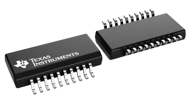
The SN54LVCH244A octal buffer/line driver is designed for 2.7-V to 3.6-V VCC operation, and the SN74LVCH244A octal buffer/line driver is designed for 1.65-V to 3.6-V VCC operation.
These devices are organized as two 4-bit line drivers with separate output-enable (OE) inputs. When OE is low, these devices pass data from the A inputs to the Y outputs. When OE is high, the outputs are in the high-impedance state.
Active bus-hold circuitry holds unused or undriven inputs at a valid logic state. Use of pullup or pulldown resistors with the bus-hold circuitry is not recommended.
Inputs can be driven from either 3.3-V or 5-V devices. This feature allows the use of these devices as translators in a mixed 3.3-V/5-V system environment.
These devices are fully specified for partial-power-down applications using Ioff. The Ioff circuitry disables the outputs, preventing damaging current backflow through the devices when they are powered down.
To ensure the high-impedance state during power up or power down, OE should be tied to VCC through a pullup resistor; the minimum value of the resistor is determined by the current-sinking capability of the driver.


