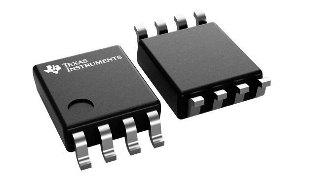
| Number of channels (#) | 2 |
| Technology Family | AUP |
| Supply voltage (Min) (V) | 0.8 |
| Supply voltage (Max) (V) | 3.6 |
| Input type | Standard CMOS |
| Output type | Push-Pull |
| Clock Frequency (Max) (MHz) | 260 |
| IOL (Max) (mA) | 4 |
| IOH (Max) (mA) | -4 |
| ICC (Max) (uA) | 0.9 |
| Features | Balanced outputs, Very high speed (tpd 5-10ns), Over-voltage tolerant inputs, Partial power down (Ioff) |
- Available in the Texas Instruments NanoStar? Package
- Low Static-Power Consumption
(ICC = 0.9 μA Maximum) - Low Dynamic-Power Consumption
(Cpd = 4.3 pF Typ at 3.3 V) - Low Input Capacitance (Ci = 1.5 pF Typical)
- Low Noise – Overshoot and Undershoot
<10% of VCC - Ioff Supports Partial-Power-Down Mode Operation
- Wide Operating VCC Range of 0.8 V to 3.6 V
- Optimized for 3.3-V Operation
- 3.6-V I/O Tolerant to Support Mixed-Mode Signal Operation
- tpd = 4.4 ns Maximum at 3.3 V
- Suitable for Point-to-Point Applications
- Latch-Up Performance Exceeds 100 mA Per JESD 78, Class II
- ESD Performance Tested Per JESD 22
- 2000-V Human-Body Model
(A114-B, Class II) - 1000-V Charged-Device Model (C101)
- 2000-V Human-Body Model
The AUP family is TI?s premier solution to the industry?s low-power needs in battery-powered portable applications. This family ensures a very low static- and dynamic-power consumption across the entire VCC range of 0.8 V to 3.6 V, resulting in increased battery life (see Figure 1). This product also maintains excellent signal integrity (see the very low undershoot and overshoot characteristics shown in Figure 2).
When data at the data (D) input meets the setup time requirement, the data is transferred to the Q output on the positive-going edge of the clock pulse. Clock triggering occurs at a voltage level and is not directly related to the rise time of the clock pulse. Following the hold-time interval, data at the D input can be changed without affecting the levels at the outputs.
NanoStar? package technology is a major breakthrough in IC packaging concepts, using the die as the package.
This device is fully specified for partial-power-down applications using Ioff. The Ioff circuitry disables the outputs, preventing damaging current backflow through the device when it is powered down.


