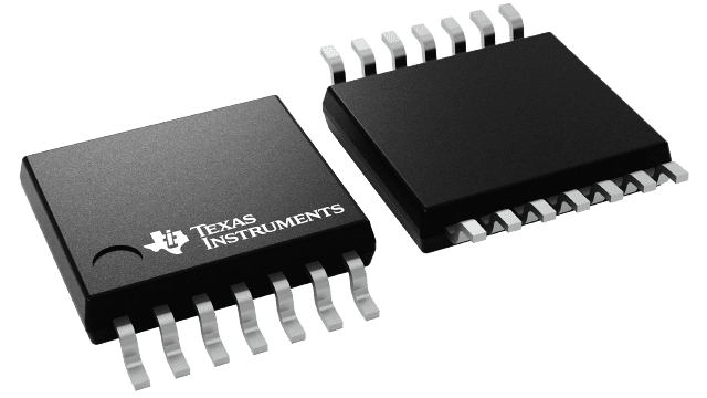
具有清零和预置端的双路正边沿触发式 D 型触发器
| Number of channels (#) | 2 |
| Technology Family | AHC |
| Supply voltage (Min) (V) | 2 |
| Supply voltage (Max) (V) | 5.5 |
| Input type | Standard CMOS |
| Output type | Push-Pull |
| Clock Frequency (Max) (MHz) | 110 |
| IOL (Max) (mA) | 8 |
| IOH (Max) (mA) | -8 |
| ICC (Max) (uA) | 20 |
| Features | Balanced outputs, High speed (tpd 10-50ns), Over-voltage tolerant inputs |
- Operating Range 2-V to 5.5-V VCC
- Latch-Up Performance Exceeds 250 mA Per JESD 17
- ESD Protection Exceeds JESD 22
- 2000-V Human-Body Model (A114-A)
- 200-V Machine Model (A115-A)
- 1000-V Charged-Device Model (C101)
The ’AHC74 dual positive-edge-triggered devices are D-type flip-flops.
A low level at the preset (PRE) or clear (CLR) inputs sets or resets the outputs, regardless of the levels of the other inputs. When PRE and CLR are inactive (high), data at the data (D) input meeting the setup time requirements is transferred to the outputs on the positive-going edge of the clock pulse. Clock triggering occurs at a voltage level and is not directly related to the rise time of the clock pulse. Following the hold-time interval, data at the D input can be changed without affecting the levels at the outputs.


