| Number of channels (#) | 2 |
| Supply voltage (Min) (V) | 2 |
| Supply voltage (Max) (V) | 6 |
| Technology Family | HC |
| Input type | Standard CMOS |
| Output type | Push-Pull |
| ICC (uA) | 80 |
| IOL (Max) (mA) | 5.2 |
| IOH (Max) (mA) | -5.2 |
| Features | Balanced outputs, High speed (tpd 10-50ns), Positive input clamp diode, Retriggerable |
- Qualified for Automotive Applications
- Retriggerable/Resettable Capability
- Trigger and Reset Propagation Delays Independent of RX, CX
- Triggering From the Leading or Trailing Edge
- Q and Q Buffered Outputs Available
- Separate Resets
- Wide Range of Output Pulse Widths
- Schmitt-Trigger Input on A and B Inputs
- Retrigger Time Is Independent of CX
- Fanout (Over Temperature Range)
- Standard Outputs . . . 10 LSTTL Loads
- Bus Driver Outputs . . . 15 LSTTL Loads
- Balanced Propagation Delay and Transition Times
- Significant Power Reduction Compared to LSTTL Logic ICs
- VCC Voltage = 2 V to 6 V
- High Noise Immunity NIL or NIH = 30% of VCC, VCC = 5 V
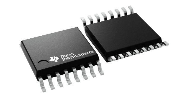
The CD74HC4538 is a dual retriggerable/resettable precision monostable multivibrator for fixed-voltage timing applications. An external resistor (RX) and external capacitor (CX) control the timing and accuracy for the circuit. Adjustment of RX and CX provides a wide range of output pulse widths from the Q and Q\ terminals. The propagation delay from trigger input-to-output transition and the propagation delay from reset input-to-output transition are independent of RX and CX.
Leading-edge triggering (A) and trailing-edge triggering (B) inputs are provided for triggering from either edge of the input pulse. An unused A input should be tied to GND and an unused B input should be tied to VCC. On power up, the IC is reset. Unused resets and sections must be terminated. In normal operation, the circuit retriggers on the application of each new trigger pulse. To operate in the nontriggerable mode, Q is connected to B\ when leading-edge triggering (A) is used, or Q is connected to A when trailing-edge triggering (B) is used. The period τ can be calculated from τ = (0.7) RX, CX; RMIN is 5 kΩ. CMIN is 0 pF.


