| Display type | LCD unipolar |
| IC integration | LCD bias |
| Vin (Min) (V) | 6 |
| Vin (Max) (V) | 14 |
| Source driver voltage (Max) (V) | 19 |
| Level shifter/scan driver (ch) | 0 |
| V_POS (Max) (V) | 30 |
| V_NEG (Max) (V) | -2 |
| Features | GPM or GVS, Output discharge, Temperature sensor or compensation |
| Topology | Boost |
| Rating | Catalog |
- 6 V to 14 V Input Voltage Range
- Vs Output Voltage Range up to 19 V
- Boost Converter With 3.5-A Switch Current
- Boost Converter Overvoltage Protection
- 2.5-A Step-Down Converter With 3.3-V Fixed or Adjustable Output
- 750 kHz Fixed Switching Frequency
- 150 mA Negative Charge Pump Driver for VGL
- 50 mA Positive Charge Pump for VGH
- LDO Controller for Logic Supply
- Gate Voltage Shaping for VGH
- Temperature Sensor Output
- TPS65167 - High Voltage Stress Test Vs
and VGH - TPS65167A - High Voltage Stress Test Vs only
- Adjustable Sequencing
- Gate Drive Signal for Isolation Switch
- Short-Circuit Protection
- Internal Soft-start
- Thermal Shutdown
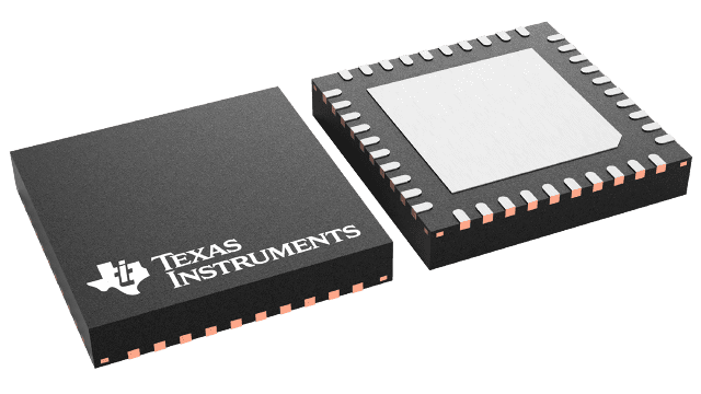
- Available in 6 × 6 mm 40 Pin QFN Package
- APPLICATIONS
- LCD TV Panel
- LCD Monitor
The TPS65167 offers a compact power supply solution to provide all voltages required by a LCD panel for large size monitor and TV panel applications running from a 12-V supply rail.
The device generates all 3 voltage rails for the TFT LCD bias (Vs, VGL and VGH). In addition to that it includes a step-down converter and a LDO controller to provide two logic voltage rails. The device incorporates a high voltage switch that can be controlled by a logic signal from the external timing controller (TCON). This function allows gate voltage shaping for VGH. The device also features a high voltage stress test where the output voltage of VGH is set to typically 30 V and the output voltage of Vs is programmable to any higher voltage. The high voltage stress test is enabled by pulling the HVS pin high. The device consists of a boost converter to provide the source voltage Vs operating at a fixed switching frequency of 750 kHz. A fully integrated positive charge pump, switching automatically between doubler and tripler mode provides an adjustable regulated TFT gate on voltage VGH. A negative charge pump driver provides adjustable regulated output voltages VGL. To minimize external components the charge pumps for VGH and VGL operate at a fixed switching frequency of 1.5 MHz. The device includes safety features like overvoltage protection of the boost converter, short-circuit protection of VGH and VGL as well as thermal shutdown.


