| Display type | LCD unipolar |
| IC integration | LCD bias |
| Vin (Min) (V) | 8 |
| Vin (Max) (V) | 14.7 |
| Source driver voltage (Max) (V) | 19 |
| Level shifter/scan driver (ch) | 0 |
| V_POS (Max) (V) | 34 |
| V_NEG (Max) (V) | -2 |
| Features | VCOM or op amp |
| Topology | Boost, Buck |
| Rating | Catalog |
- 8-V to 14.7-V Input Voltage Range
- 500 kHz / 750 kHz Fixed Switching Frequency
- Boost Output Voltage up to 19 V
- 1%-Accurate Boost With 2.8-A Switch Current Overvoltage Protection
- Input-to-Output Isolation Switch for Vs Short-Circuit protection for Boost
- 2.5-A Step-Down Converter
- Regulated Positive Charge-Pump Driver VGH
- Regulated Negative Charge-Pump Driver VGL
- Gate Voltage Shaping for VGH
- Soft Start for all Converters
- Two Integrated High-Speed Opamps
- 50-MHz, 3-dB Bandwidth
- Slew Rate 55 V / μs
- 215-mA Short-Circuit Current
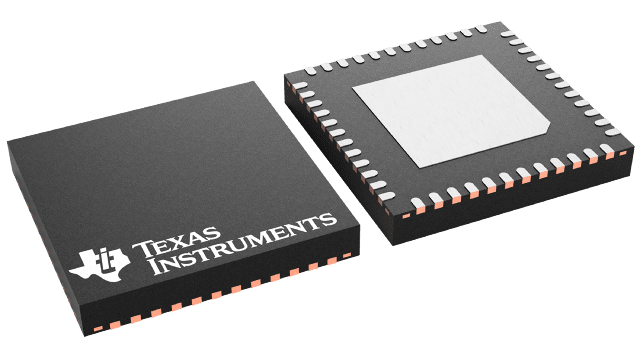
- 48 Pin 7x7 mm QFN Package
The TPS65162 is a compact LCD bias IC with two high-speed operational amplifiers for the Vcom supply. The high current capability of the device is ideal for large LCD-monitor and LCD-TV applications.
The TPS65162 generates all four voltage rails for a TFT LCD (Vs, Vlogic, VGH and VGL) and includes two op-amps to generate the VCOM supply rail. An input-to-output isolation switch is integrated into the device, providing short-circuit protection for the boost converter. A current-limit function is implemented in the input-to-output isolation switch to allow soft turn-on during start-up. The device also features gate voltage shaping for improved TFT-LCD picture quality. The device consists of a boost converter to provide the source voltage Vs, and a step-down converter to provide the logic voltage for the system. A positive and a negative charge-pump driver provide adjustable regulated output voltages VGH and VGL to bias the TFT. Both boost and buck converter, as well as the charge-pump drivers, operate with a fixed switching frequency of 500 kHz or 750 kHz, selectable by the FREQ pin. The device includes adjustable power-on sequencing. The safety features of the device are overvoltage protection for boost converter, short-circuit protection for Vs, Vlogic and VGH, and thermal shutdown.


