| Output options | Adjustable Output, Fixed Output |
| Iout (Max) (A) | 1 |
| Vin (Max) (V) | 10 |
| Vin (Min) (V) | 2.7 |
| Vout (Max) (V) | 5.5 |
| Vout (Min) (V) | 1.2 |
| Fixed output options (V) | 1.5, 1.8, 2.5, 2.7, 2.8, 3, 3.3, 5 |
| Noise (uVrms) | 55 |
| Iq (Typ) (mA) | 0.08 |
| Thermal resistance θJA (°C/W) | 33 |
| Rating | Catalog |
| Load capacitance (Min) (μF) | 10 |
| Regulated outputs (#) | 1 |
| Features | Enable, Power good |
| Accuracy (%) | 2 |
| PSRR @ 100 KHz (dB) | 29 |
| Dropout voltage (Vdo) (Typ) (mV) | 230 |
| Operating temperature range (C) | -40 to 125 |
- Input Voltage Range: 2.7 V to 10 V
- Low-Dropout Voltage: 230 mV typical at 1 A (TPS76850)
- 2% Tolerance Over Specified Conditions for Fixed-Output Versions
- Open Drain Power Good (See TPS767xx for Power-On Reset With 200-ms Delay Option)
- Ultralow 85 μA Typical Quiescent Current
- Available in 1.5-V, 1.8-V, 2.5-V, 2.7-V, 2.8-V, 3.0-V, 3.3-V, 5.0-V Fixed Output and Adjustable (1.2 V to 5.5 V) Versions
- Fast Transient Response
- Thermal Shutdown Protection
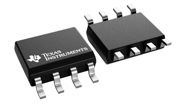
- SOIC-8 (D) and TSSOP-20 (PWP) Package
All trademarks are the property of their respective owners.
This device is designed to have a fast transient response and be stable with 10 μF capacitors. This combination provides high performance at a reasonable cost.
Since the PMOS device behaves as a low-value resistor, the dropout voltage is very low (typically 230 mV at an output current of 1 A for the TPS76850) and is directly proportional to the output current. Additionally, because the PMOS pass element is a voltage-driven device, the quiescent current is very low and independent of output loading (typically 85 μA over the full range of output current, 0 mA to 1 A). These two key specifications yield a significant improvement in operating life for battery-powered systems. This LDO family also features a shutdown mode; applying a TTL high signal to EN (enable) shuts down the regulator, reducing the quiescent current to less than 1 μA at TJ = 25°C.
Power good (PG) is an active high output, which can be used to implement a power-on reset or a low-battery indicator.


